ZHCSJN9E january   2019  – april 2023 DLPC3436

PRODUCTION DATA  

  1.   1
  2. 特性
  3. 应用
  4. 说明
  5. Revision History
  6. Pin Configuration and Functions
    1. 5.1 Test Pins and General Control
    2. 5.2 Parallel Port Input
    3. 5.3 DSI Input Data and Clock
    4. 5.4 DMD Reset and Bias Control
    5. 5.5 DMD Sub-LVDS Interface
    6. 5.6 Peripheral Interface
    7. 5.7 GPIO Peripheral Interface
    8. 5.8 Clock and PLL Support
    9. 5.9 Power and Ground
  7. Specifications
    1. 6.1  Absolute Maximum Ratings
    2. 6.2  ESD Ratings
    3. 6.3  Recommended Operating Conditions
    4. 6.4  Thermal Information
    5. 6.5  Power Electrical Characteristics
    6. 6.6  Pin Electrical Characteristics
    7. 6.7  Internal Pullup and Pulldown Electrical Characteristics
    8. 6.8  DMD Sub-LVDS Interface Electrical Characteristics
    9. 6.9  DMD Low-Speed Interface Electrical Characteristics
    10. 6.10 System Oscillator Timing Requirements
    11. 6.11 Power Supply and Reset Timing Requirements
    12. 6.12 Parallel Interface Frame Timing Requirements
    13. 6.13 Parallel Interface General Timing Requirements
    14. 6.14 Flash Interface Timing Requirements
    15. 6.15 Other Timing Requirements
    16. 6.16 DMD Sub-LVDS Interface Switching Characteristics
    17. 6.17 DMD Parking Switching Characteristics
    18. 6.18 Chipset Component Usage Specification
  8. Detailed Description
    1. 7.1 Overview
    2. 7.2 Functional Block Diagram
    3. 7.3 Feature Description
      1. 7.3.1 Input Source Requirements
        1. 7.3.1.1 Input Frame Rates and 3-D Display Operation
          1. 7.3.1.1.1 Parallel Interface Data Transfer Format
        2. 7.3.1.2 3D Display
      2. 7.3.2 Device Startup
      3. 7.3.3 SPI Flash
        1. 7.3.3.1 SPI Flash Interface
        2. 7.3.3.2 SPI Flash Programming
      4. 7.3.4 I2C Interface
      5. 7.3.5 Content Adaptive Illumination Control (CAIC)
      6. 7.3.6 Local Area Brightness Boost (LABB)
      7. 7.3.7 3D Glasses Operation
      8. 7.3.8 Test Point Support
      9. 7.3.9 DMD Interface
        1. 7.3.9.1 Sub-LVDS (HS) Interface
    4. 7.4 Device Functional Modes
    5. 7.5 Programming
  9. Application and Implementation
    1. 8.1 Application Information
    2. 8.2 Typical Application
      1. 8.2.1 Design Requirements
      2. 8.2.2 Detailed Design Procedure
      3. 8.2.3 Application Curve
  10. Power Supply Recommendations
    1. 9.1 PLL Design Considerations
    2. 9.2 System Power-Up and Power-Down Sequence
    3. 9.3 Power-Up Initialization Sequence
    4. 9.4 DMD Fast Park Control (PARKZ)
    5. 9.5 Hot Plug I/O Usage
    6. 9.6 Maximum Signal Transition Time
  11. 10Layout
    1. 10.1 Layout Guidelines
      1. 10.1.1 PLL Power Layout
      2. 10.1.2 Reference Clock Layout
        1. 10.1.2.1 Recommended Crystal Oscillator Configuration
      3. 10.1.3 Unused Pins
      4. 10.1.4 DMD Control and Sub-LVDS Signals
      5. 10.1.5 Layer Changes
      6. 10.1.6 Stubs
      7. 10.1.7 Terminations
      8. 10.1.8 Routing Vias
      9. 10.1.9 Thermal Considerations
    2. 10.2 Layout Example
  12. 11Device and Documentation Support
    1. 11.1 Device Support
      1. 11.1.1 第三方米6体育平台手机版_好二三四免责声明
      2. 11.1.2 Device Nomenclature
        1. 11.1.2.1 Device Markings DLPC343x
        2. 11.1.2.2 Device Markings DLPC342x
        3. 11.1.2.3 Video Timing Parameter Definitions
    2. 11.2 Documentation Support
      1. 11.2.1 Related Documentation
    3. 11.3 Related Links
    4. 11.4 接收文档更新通知
    5. 11.5 支持资源
    6. 11.6 Trademarks
    7. 11.7 静电放电警告
    8. 11.8 术语表
  13. 12Mechanical, Packaging, and Orderable Information
    1. 12.1 Package Option Addendum
      1. 12.1.1 Packaging Information

封装选项

机械数据 (封装 | 引脚)
散热焊盘机械数据 (封装 | 引脚)
订购信息

Typical Application

A typical application when using a DLPC34x6 controller with a DLP230NP/NPSE (.23 Full HD) and a DLPA200x or DLPA300x PMIC/LED driver is to create a Pico projector embedded in a handheld product. For example, a Pico projector may be embedded in a smartphone, tablet, camera, or camcorder. The controller in the Pico projector embedded module typically receives images from a host processor within the product.
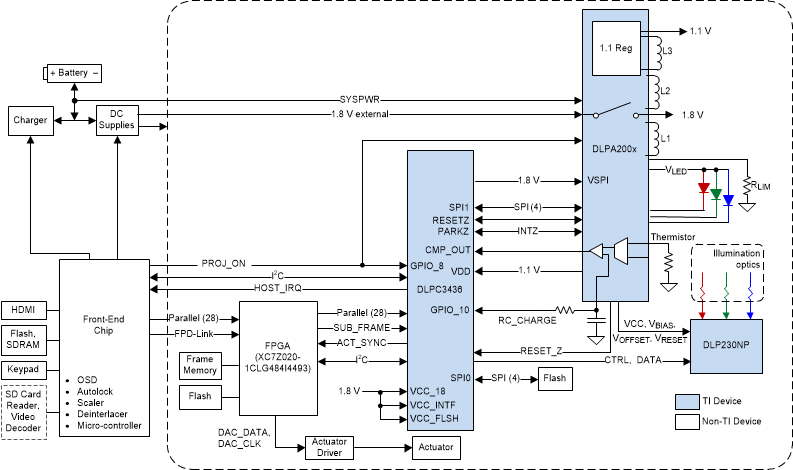
GUID-8E2E7653-95C0-46CE-84F2-445DCA7A0EC2-low.gif Figure 8-1 Typical Application Diagram (using DLPA200x)
GUID-20200909-CA0I-JQWN-RDHN-GR1ZGK601HJJ-low.svg Figure 8-2 Typical Application Diagram (using DLPA300x)