ZHCSCU2E February 2014 – November 2020 DLPC3433 , DLPC3438
PRODUCTION DATA
- 1 特性
- 2 应用
- 3 说明
- 4 Revision History
- 5 Pin Configuration and Functions
-
6 Specifications
- 6.1 Absolute Maximum Ratings
- 6.2 ESD Ratings
- 6.3 Recommended Operating Conditions
- 6.4 Thermal Information
- 6.5 Power Electrical Characteristics
- 6.6 Pin Electrical Characteristics
- 6.7 Internal Pullup and Pulldown Electrical Characteristics
- 6.8 DMD Sub-LVDS Interface Electrical Characteristics
- 6.9 DMD Low-Speed Interface Electrical Characteristics
- 6.10 System Oscillator Timing Requirements
- 6.11 Power Supply and Reset Timing Requirements
- 6.12 Parallel Interface Frame Timing Requirements
- 6.13 Parallel Interface General Timing Requirements
- 6.14 BT656 Interface General Timing Requirements
- 6.15 DSI Host Timing Requirements
- 6.16 Flash Interface Timing Requirements
- 6.17 Other Timing Requirements
- 6.18 DMD Sub-LVDS Interface Switching Characteristics
- 6.19 DMD Parking Switching Characteristics
- 6.20 Chipset Component Usage Specification
-
7 Detailed Description
- 7.1 Overview
- 7.2 Functional Block Diagram
- 7.3 Feature Description
- 7.4 Device Functional Modes
- 7.5 Programming
- 8 Application and Implementation
- 9 Power Supply Recommendations
- 10Layout
- 11Device and Documentation Support
- 12Mechanical, Packaging, and Orderable Information
9.2 System Power-Up and Power-Down Sequence
Although the DLPC34xx controller requires an array of power supply voltage pins (for example, VDD, VDDLP12, VDD_PLLM/D, VCC18, VCC_FLSH, and VCC_INTF), if VDDLP12 is tied to the 1.1-V VDD supply (which is assumed to be the typical configuration), then there are no restrictions regarding the relative order of power supply sequencing to avoid damaging the DLPC34xx controller (this remains true for both power-up and power-down scenarios). The controller requires no minimum delay time between powering-up and powering-down the individual supplies if the VDDLP12 is tied to the 1.1-V VDD supply.
However, if the VDDLP12 pin is not tied to the VDD supply, then the VDDLP12 pin must be powered-on only after the VDD supply is powered-on. And in a similar sequence, the VDDLP12 pin must be powered-off before the VDD supply is powered-off. If the VDDLP12 pin is not tied to VDD, then the VDDLP12 pin and VDD supply pins must be powered-on or powered-off within 100 ms of each other.
Although there is no risk of damaging the DLPC34xx controller when the above power sequencing rules are followed, these additional power sequencing recommendations must be considered to ensure proper system operation:
- To ensure that the DLPC34xx controller output signal states behave as expected, all controller I/O supplies are encouraged to remain applied while VDD core power is applied. If VDD core power is removed while the I/O supply (VCC_INTF) is applied, then the output signal states associated with the inactive I/O supply go to a high impedance state.
- Because additional power sequencing rules may exist for devices that share the supplies with the DLPC34xx controller (such as the PMIC and DMD), these devices may force additional system power sequencing requirements.
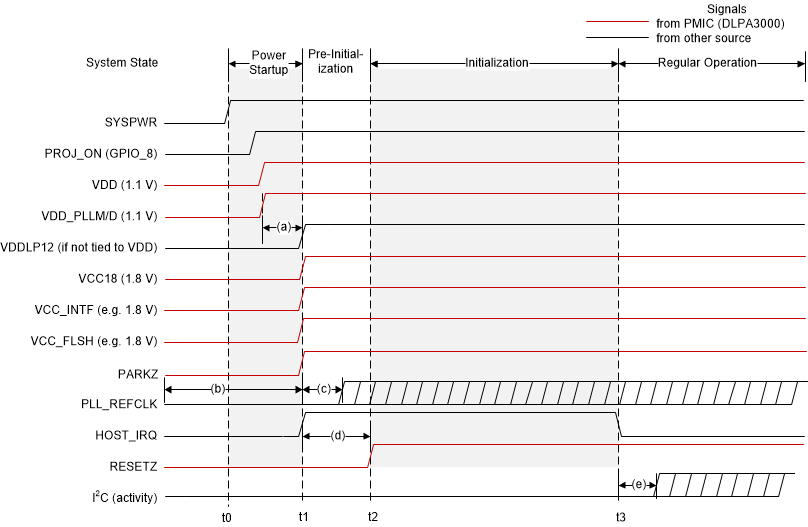
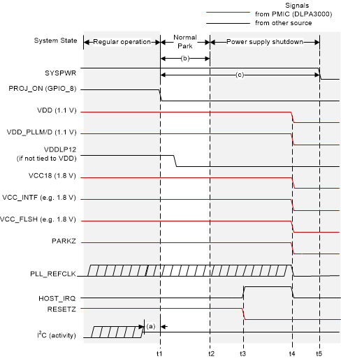
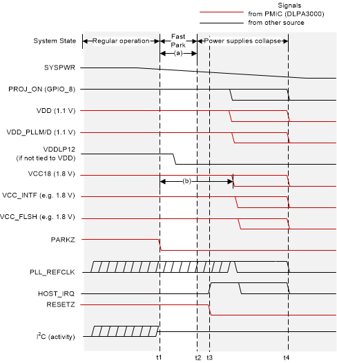
Figure 9-1, Figure 9-2, and Figure 9-3 show the DLPC34xx power-up sequence, the normal PARK power-down sequence, and the fast PARK power-down sequence of a typical DLPC34xx system.
When the VDD core power is applied, but I/O power is not applied, the controller may draw additional leakage current. This leakage current does not affect the normal DLPC34xx controller operation or reliability.
During a Normal Park it is recommended to maintain SYSPWR within specification for at least 50 ms after PROJ_ON goes low. This is to allow the DMD to be parked and the power supply rails to safely power down. After 50 ms, SYSPWR can be turned off. If a DLPA200x is used, it is also recommended that the 1.8-V supply fed into the DLPA200x load switch be maintained within specification for at least 50 ms after PROJ_ON goes low.

| t0: | SYSPWR applied to the PMIC. All other voltage rails are derived from SYSPWR. |
| t1: | All supplies reach 95% of their specified nominal value. Note HOST_IRQ may go high sooner if it is pulled-up to a different external supply. |
| t2: | Point where RESETZ is deasserted (goes high). This indicates the beginning of the controller auto-initialization routine. |
| t3: | HOST_IRQ goes low to indicate initialization is complete. |
| (a): | VDDLP12 must be powered on after VDD if it is supplied from a separate source. |
| (b): | PLL_REFCLK is allowed to be active before power is applied. |
| (c): | PLL_REFCLK must be stable within 5 ms of all power being applied. For external oscillator applications this is oscillator dependent, and for crystal applications this is crystal and controller oscillator cell dependent. |
| (d): | PARKZ must be high before RESETZ releases to support auto-initialization. RESETZ must also be held low for at least 5 ms after the power supplies are in specification. |
| (e): | I2C activity cannot start until HOST_IRQ goes low to indicate auto-initialization completes. |

| t1: | PROJ_ON goes low to begin the power down sequence. |
| t2: | The controller finishes parking the DMD. |
| t3: | RESETZ is asserted which causes HOST_IRQ to be pulled high. |
| t4: | All controller power supplies are turned off. |
| t5: | SYSPWR is removed now that all other supplies are turned off. |
| (a): | I2C activity must stop before PROJ_ON is deasserted (goes low). |
| (b): | The DMD will be parked within 20 ms of PROJ_ON being deasserted (going low). VDD, VDD_PLLM/D, VCC18, VCC_INITF, and VCC_FLSH power supplies and the PLL_REFCLK must be held within specification for a minimum of 20 ms after PROJ_ON is deasserted (goes low). However, 20 ms does not satisfy the typical shutdown timing of the entire chipset. It is therefore recommended to follow note (c). |
| (c): | It is recommended that SYSPWR not be turned off for 50 ms after PROJ_ON is deasserted (goes low). This time allows the DMD to be parked, the controller to turn off, and the PMIC supplies to shut down. |

| t1: | A fault is detected (in this example the PMIC detects a UVLO condition) and PARKZ is asserted (goes low) to tell the controller to initiate a fast park of the DMD. |
| t2: | The controller finishes the fast park procedure. |
| t3: | RESETZ is asserted which puts the controller in a reset state which causes HOST_IRQ to be pulled high. |
| t4: | Eventually all power supplies that were derived from SYSPWR collapse. |
| (a): | VDD, VDD_PLLM/D, VCC18, VCC_INITF, and VCC_FLSH power supplies and the PLL_REFCLK must be held within specification for a minimum of 32 µs after PARKZ is asserted (goes low). |
| (b): | VCC18 must remain in specification long enough to satisfy DMD power sequencing requirements defined in the DMD datasheet. Also see the DLPAxxxx datasheets for more information. |