ZHCSCU2E February 2014 – November 2020 DLPC3433 , DLPC3438
PRODUCTION DATA
- 1 特性
- 2 应用
- 3 说明
- 4 Revision History
- 5 Pin Configuration and Functions
-
6 Specifications
- 6.1 Absolute Maximum Ratings
- 6.2 ESD Ratings
- 6.3 Recommended Operating Conditions
- 6.4 Thermal Information
- 6.5 Power Electrical Characteristics
- 6.6 Pin Electrical Characteristics
- 6.7 Internal Pullup and Pulldown Electrical Characteristics
- 6.8 DMD Sub-LVDS Interface Electrical Characteristics
- 6.9 DMD Low-Speed Interface Electrical Characteristics
- 6.10 System Oscillator Timing Requirements
- 6.11 Power Supply and Reset Timing Requirements
- 6.12 Parallel Interface Frame Timing Requirements
- 6.13 Parallel Interface General Timing Requirements
- 6.14 BT656 Interface General Timing Requirements
- 6.15 DSI Host Timing Requirements
- 6.16 Flash Interface Timing Requirements
- 6.17 Other Timing Requirements
- 6.18 DMD Sub-LVDS Interface Switching Characteristics
- 6.19 DMD Parking Switching Characteristics
- 6.20 Chipset Component Usage Specification
-
7 Detailed Description
- 7.1 Overview
- 7.2 Functional Block Diagram
- 7.3 Feature Description
- 7.4 Device Functional Modes
- 7.5 Programming
- 8 Application and Implementation
- 9 Power Supply Recommendations
- 10Layout
- 11Device and Documentation Support
- 12Mechanical, Packaging, and Orderable Information
7.3.1.3.1 PDATA Bus – Parallel Interface Bit Mapping Modes
 Figure 7-2 RGB-888 and YCbCr-888 I/O Mapping
 Figure 7-3 RGB-666 and YCbCr-666 I/O Mapping
 Figure 7-4 RGB-565 and YCbCr-565 I/O Mapping
 Figure 7-5 16-Bit YCbCr-880 I/O Mapping
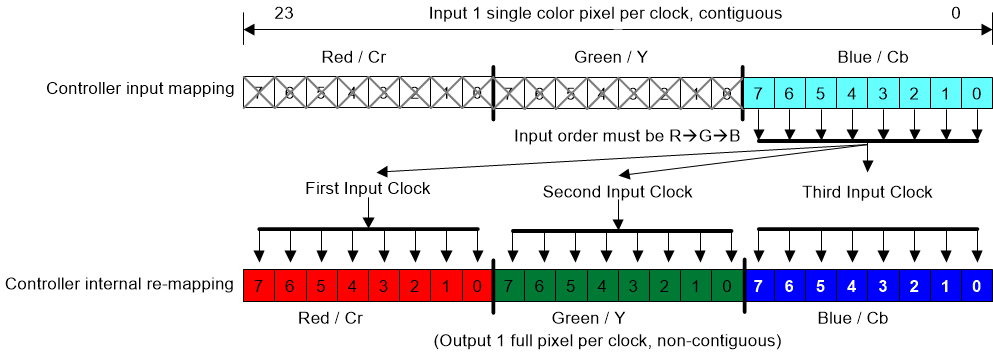
 Figure 7-6 8-Bit RGB-888 or YCbCr-888 I/O Mapping
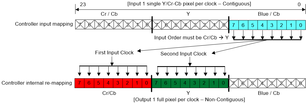
 Figure 7-7 8-Bit Serial YCbCr-422 I/O Mapping