ZHCSCU2E February 2014 – November 2020 DLPC3433 , DLPC3438
PRODUCTION DATA
- 1 特性
- 2 应用
- 3 说明
- 4 Revision History
- 5 Pin Configuration and Functions
-
6 Specifications
- 6.1 Absolute Maximum Ratings
- 6.2 ESD Ratings
- 6.3 Recommended Operating Conditions
- 6.4 Thermal Information
- 6.5 Power Electrical Characteristics
- 6.6 Pin Electrical Characteristics
- 6.7 Internal Pullup and Pulldown Electrical Characteristics
- 6.8 DMD Sub-LVDS Interface Electrical Characteristics
- 6.9 DMD Low-Speed Interface Electrical Characteristics
- 6.10 System Oscillator Timing Requirements
- 6.11 Power Supply and Reset Timing Requirements
- 6.12 Parallel Interface Frame Timing Requirements
- 6.13 Parallel Interface General Timing Requirements
- 6.14 BT656 Interface General Timing Requirements
- 6.15 DSI Host Timing Requirements
- 6.16 Flash Interface Timing Requirements
- 6.17 Other Timing Requirements
- 6.18 DMD Sub-LVDS Interface Switching Characteristics
- 6.19 DMD Parking Switching Characteristics
- 6.20 Chipset Component Usage Specification
-
7 Detailed Description
- 7.1 Overview
- 7.2 Functional Block Diagram
- 7.3 Feature Description
- 7.4 Device Functional Modes
- 7.5 Programming
- 8 Application and Implementation
- 9 Power Supply Recommendations
- 10Layout
- 11Device and Documentation Support
- 12Mechanical, Packaging, and Orderable Information
7.3.7 3D Glasses Operation
When using 3D glasses (with 3D video input and appropriate software support), the controller outputs sync information to align the left eye and right eye shuttering in the glasses with the displayed DMD image frames. 3D glasses typically use either Infrared (IR) transmission or DLP Link™ technology to achieve this synchronization.
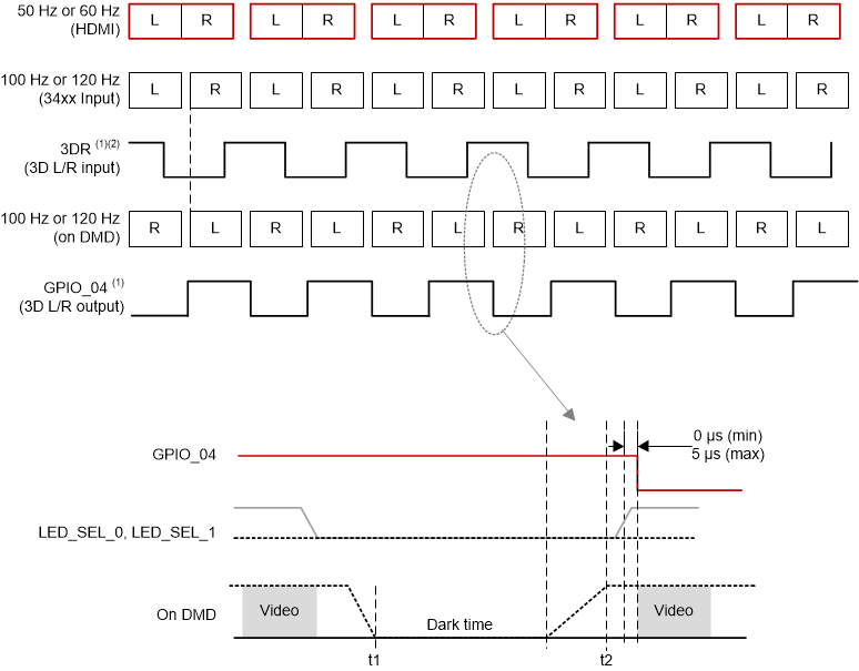
One glasses type uses an IR transmitter on the system PCB to send an IR sync signal to an IR receiver in the glasses. In this case DLPC34xx controller output signal GPIO_04 can be used to cause the IR transmitter to send an IR sync signal to the glasses. The Figure 7-14 figure shows the timing sequence for the GPIO_04 signal.
The second type of glasses relies on sync information that is encoded into the light being output from the projection lens. This approach uses the DLP Link feature for 3D video. Many 3D glasses from different suppliers have been built using this method. The advantage of using the DLP Link feature is that it takes advantage of existing projector hardware to transmit the sync information to the glasses. This method may give an advantage in cost, size and power savings in the projector.
When using DLP Link technology, one light pulse per DMD frame is output from the projection lens while the glasses have both shutters closed. To achieve this, the DLPC34xx tells the DLPAxxxx when to turn on the illumination source (typically LEDs or lasers) so that an encoded light pulse is output once per DMD frame. Because the shutters in the glasses are both off when the pulse is sent, the projector illumination source is also off except when the light is sent to create the pulse. The pulses may use any color; however, due to the transmission property of the eye-glass LCD shutter lenses and the sensitivity of the white-light sensor used on the eye-glasses, it is highly recommended that blue is not used for pulses. Red pulses are the recommended color to use. The Figure 7-14 figure below shows 3D timing information. Figure 7-15 and Table 7-7 show the timing for the light pulses when using the DLP Link feature.


| HDMI Source Frame Rate (Hz)(1) | DLPC34xx Input Frame Rate (Hz) | A (µs) |
B (µs) |
C (µs) |
D (µs) |
E (µs) |
|---|---|---|---|---|---|---|
| 49.0 | 98 | 20 - 32 (31.8 nominal) |
> 500 | > 622 | 128 - 163 (161.6 nominal) |
> 2000 |
| 50.0 | 100 | 20 - 32 (31.2 nominal) |
> 500 | > 658 | 128 - 163 (158.4 nominal) |
> 2000 |
| 51.0 | 102 | 20 - 32 (30.6 nominal) |
> 500 | > 655 | 128 - 163 (155.3 nominal) |
> 2000 |
| 59.0 | 118 | 20 - 32 (26.4 nominal) |
> 500 | > 634 | 128 - 163 (134.2 nominal) |
> 2000 |
| 60.0 | 120 | 20 - 32 (26.0 nominal) |
> 500 | > 632 | 128 - 163 (132.0 nominal) |
> 2000 |
| 61.0 | 122 | 20 - 32 (25.6 nominal) |
> 500 | > 630 | 128 - 163 (129.8 nominal) |
> 2000 |