ZHCSHY3C April   2018  – December 2020 DLPC3478

PRODUCTION DATA  

  1. 特性
  2. 应用
  3. 说明
  4. Revision History
  5. Pin Configuration and Functions
  6. Specifications
    1. 6.1  Absolute Maximum Ratings
    2. 6.2  ESD Ratings
    3. 6.3  Recommended Operating Conditions
    4. 6.4  Thermal Information
    5. 6.5  Power Electrical Characteristics
    6. 6.6  Pin Electrical Characteristics
    7. 6.7  Internal Pullup and Pulldown Electrical Characteristics
    8. 6.8  DMD Sub-LVDS Interface Electrical Characteristics
    9. 6.9  DMD Low-Speed Interface Electrical Characteristics
    10. 6.10 System Oscillator Timing Requirements
    11. 6.11 Power Supply and Reset Timing Requirements
    12. 6.12 Parallel Interface Frame Timing Requirements
    13. 6.13 Parallel Interface General Timing Requirements
    14. 6.14 BT656 Interface General Timing Requirements
    15. 6.15 Flash Interface Timing Requirements
    16. 6.16 Other Timing Requirements
    17. 6.17 DMD Sub-LVDS Interface Switching Characteristics
    18. 6.18 DMD Parking Switching Characteristics
    19. 6.19 Chipset Component Usage Specification
  7. Detailed Description
    1. 7.1 Overview
    2. 7.2 Functional Block Diagram
    3. 7.3 Feature Description
      1. 7.3.1  Input Source
        1. 7.3.1.1 Supported Resolution and Frame Rates
        2. 7.3.1.2 3D Display
        3. 7.3.1.3 Parallel Interface
          1. 7.3.1.3.1 PDATA Bus – Parallel Interface Bit Mapping Modes
      2. 7.3.2  Pattern Display
        1. 7.3.2.1 External Pattern Mode
          1. 7.3.2.1.1 8-bit Monochrome Patterns
          2. 7.3.2.1.2 1-Bit Monochrome Patterns
        2. 7.3.2.2 Internal Pattern Mode
          1. 7.3.2.2.1 Free Running Mode
          2. 7.3.2.2.2 Trigger In Mode
      3. 7.3.3  Device Startup
      4. 7.3.4  SPI Flash
        1. 7.3.4.1 SPI Flash Interface
        2. 7.3.4.2 SPI Flash Programming
      5. 7.3.5  I2C Interface
      6. 7.3.6  Content Adaptive Illumination Control (CAIC)
      7. 7.3.7  Local Area Brightness Boost (LABB)
      8. 7.3.8  3D Glasses Operation
      9. 7.3.9  Test Point Support
      10. 7.3.10 DMD Interface
        1. 7.3.10.1 Sub-LVDS (HS) Interface
    4. 7.4 Device Functional Modes
    5. 7.5 Programming
  8. Application and Implementation
    1. 8.1 Application Information
    2. 8.2 Typical Application
      1. 8.2.1 Pattern projector for 3D depth scanning
        1. 8.2.1.1 Design Requirements
        2. 8.2.1.2 Detailed Design Procedure
        3. 8.2.1.3 Application Curve
      2. 8.2.2 3D Depth Scanner Using Internal Pattern Streaming Mode
        1. 8.2.2.1 Design Requirements
        2. 8.2.2.2 Detailed Design Procedure
        3. 8.2.2.3 Application Curve
  9. Power Supply Recommendations
    1. 9.1 PLL Design Considerations
    2. 9.2 System Power-Up and Power-Down Sequence
    3. 9.3 Power-Up Initialization Sequence
    4. 9.4 DMD Fast Park Control (PARKZ)
    5. 9.5 Hot Plug I/O Usage
  10. 10Layout
    1. 10.1 Layout Guidelines
      1. 10.1.1 PLL Power Layout
      2. 10.1.2 Reference Clock Layout
        1. 10.1.2.1 Recommended Crystal Oscillator Configuration
      3. 10.1.3 Unused Pins
      4. 10.1.4 DMD Control and Sub-LVDS Signals
      5. 10.1.5 Layer Changes
      6. 10.1.6 Stubs
      7. 10.1.7 Terminations
      8. 10.1.8 Routing Vias
      9. 10.1.9 Thermal Considerations
    2. 10.2 Layout Example
  11. 11Device and Documentation Support
    1. 11.1 Device Support
      1. 11.1.1 第三方米6体育平台手机版_好二三四免责声明
      2. 11.1.2 Device Nomenclature
        1. 11.1.2.1 Device Markings
      3. 11.1.3 Video Timing Parameter Definitions
    2. 11.2 Documentation Support
      1. 11.2.1 Related Documentation
    3. 11.3 接收文档更新通知
    4. 11.4 支持资源
    5. 11.5 Trademarks
    6. 11.6 静电放电警告
    7. 11.7 术语表
  12. 12Mechanical, Packaging, and Orderable Information

封装选项

机械数据 (封装 | 引脚)
散热焊盘机械数据 (封装 | 引脚)
订购信息
Free Running Mode

In free running mode the DLPC3478 controller generates an internal synchronization signal to display pre-stored patterns. User sends an I2C command to instruct the DLPC3478 controller to download the 1D patterns from flash memory into DLPC3478 controller’s internal memory and begin display of the 1D patterns.
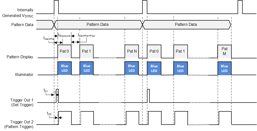
GUID-20201214-CA0I-2Q9T-HSZF-L9HDVDJFV96G-low.gif Figure 7-14 Free Running Mode

  • The device displays multiple 1D patterns within an internally-generated VSYNC period. tExposure (exposure time), tDarkPre and tDarkPost (dark time) are equal for all the 1D patterns within one internally generated VSYNC frame.
  • The Blue LED is configured to be on for each pattern.
  • TRIG_OUT_1 (Frame Trigger) is configured active high polarity and will have a minimum pulse width of 20 microseconds. TRIG_OUT_1 delay (tD1) is configured with respect to internally generated VSYNC.
  • TRIG_OUT_2 (Pattern Trigger) is configured active high polarity and stays active during the pattern exposure. TRIG_OUT_2 delay (tD2) is configured with reference to the start of each pattern.
  • VSYNC is generated internally according to different sets of patterns stored in the SPI flash memory.