ZHCSHY3C April 2018 – December 2020 DLPC3478
PRODUCTION DATA
- 1 特性
- 2 应用
- 3 说明
- 4 Revision History
- 5 Pin Configuration and Functions
-
6 Specifications
- 6.1 Absolute Maximum Ratings
- 6.2 ESD Ratings
- 6.3 Recommended Operating Conditions
- 6.4 Thermal Information
- 6.5 Power Electrical Characteristics
- 6.6 Pin Electrical Characteristics
- 6.7 Internal Pullup and Pulldown Electrical Characteristics
- 6.8 DMD Sub-LVDS Interface Electrical Characteristics
- 6.9 DMD Low-Speed Interface Electrical Characteristics
- 6.10 System Oscillator Timing Requirements
- 6.11 Power Supply and Reset Timing Requirements
- 6.12 Parallel Interface Frame Timing Requirements
- 6.13 Parallel Interface General Timing Requirements
- 6.14 BT656 Interface General Timing Requirements
- 6.15 Flash Interface Timing Requirements
- 6.16 Other Timing Requirements
- 6.17 DMD Sub-LVDS Interface Switching Characteristics
- 6.18 DMD Parking Switching Characteristics
- 6.19 Chipset Component Usage Specification
-
7 Detailed Description
- 7.1 Overview
- 7.2 Functional Block Diagram
- 7.3 Feature Description
- 7.4 Device Functional Modes
- 7.5 Programming
- 8 Application and Implementation
- 9 Power Supply Recommendations
- 10Layout
- 11Device and Documentation Support
- 12Mechanical, Packaging, and Orderable Information
7.3.2.1.2 1-Bit Monochrome Patterns
Similar to the 8-bit external pattern mode, the maximum supported 24-bit input frame for 1-bit external pattern mode is 104.2 Hz. In 1-bit pattern mode each of the 24-bit inputs are treated as separate binary patterns resulting in a maximum of 24 patterns. The maximum pattern rate for each 1-bit pattern is 2500 Hz.
The DLPC3478 controller firmware allows for the following user programmability:
- Exposure time: Time during which a pattern is displayed.
- Dark time: Time during which no pattern is displayed and the illumination in off.
- Number of 1-bit patterns within a frame - up to maximum of 24.
- Illuminator: Illuminator that is on for each 1-bit pattern. User defined illuminator is auto selected for all the patterns within a frame. User cannot select different illuminator for different 1-bit patterns within a frame.
- TRIG_OUT_1 and TRIG_OUT_2 signal configuration and delay.
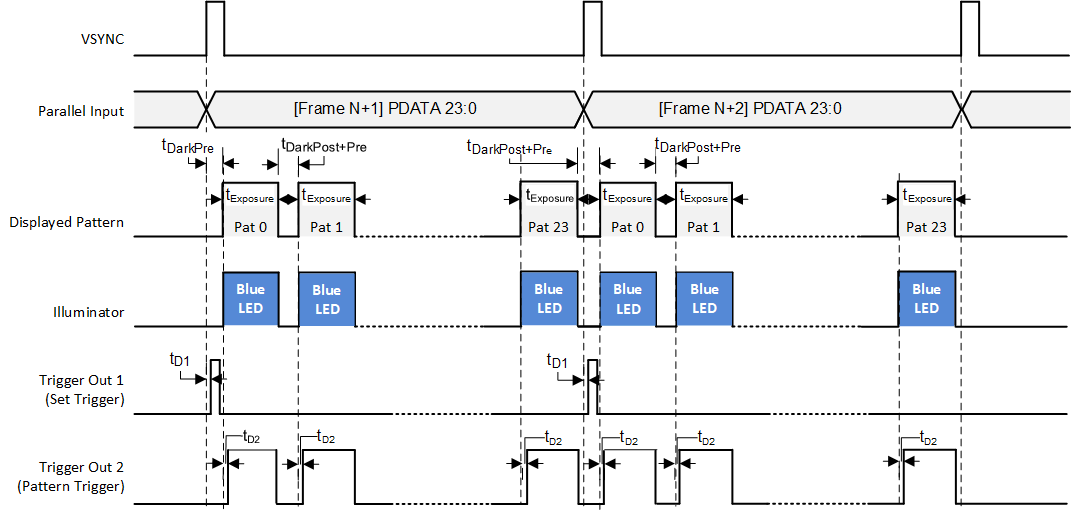
Figure 7-11 shows a configuration with 24 × 1-bit patterns.
 Figure 7-11 24 × 1-bit (Blue) Pattern
Configurations
- 24 × 1-bit patterns are displayed within each input VSYNC frame period.
- tDarkPre, tExposure and tDarkPost are the same for each pattern within a frame period.
- The sum of dark time and exposure time (tDarkPre + tExposure + tDarkPost) for all the 1-bit patterns must be equal to or less than the full frame period. If the sum is less than the full frame period, additional dark time will be appended to the end of the last pattern.
- The Blue LED is configured to be ON for each pattern.
- TRIG_OUT_1 (Frame Trigger) is configured active high polarity and will have a minimum pulse width of 20 microseconds. TRIG_OUT_1 delay (tD1) is configured with respect to input VSYNC.
- TRIG_OUT_2 (Pattern Trigger) is configured active high polarity and stays active during the pattern exposure. TRIG_OUT_2 delay (tD2) is configured with reference to the start of the pattern and is set once per pattern within a frame.