ZHCSC08C December 2013 – August 2015 DLPC6401
PRODUCTION DATA.
- 1 特性
- 2 应用
- 3 说明
- 4 修订历史记录
- 5 Pin Configuration and Functions
-
6 Specifications
- 6.1 Absolute Maximum Ratings
- 6.2 ESD Ratings
- 6.3 Recommended Operating Conditions
- 6.4 Thermal Information
- 6.5 Electrical Characteristics
- 6.6 Electrical Characteristics (Normal Mode)
- 6.7 System Oscillators Timing Requirements
- 6.8 Test and Reset Timing Requirements
- 6.9 JTAG Interface: I/O Boundary Scan Application Timing Requirements
- 6.10 Port 1 Input Pixel Interface Timing Requirements
- 6.11 Port 2 Input Pixel Interface (FPD-Link Compatible LVDS Input) Timing Requirements
- 6.12 Synchronous Serial Port (SSP) Interface Timing Requirements
- 6.13 Programmable Output Clocks Switching Characteristics
- 6.14 Synchronous Serial Port (SSP) Interface Switching Characteristics
- 6.15 JTAG Interface: I/O Boundary Scan Application Switching Characteristics
- 7 Detailed Description
- 8 Application and Implementation
- 9 Power Supply Recommendations
- 10Layout
- 11器件和文档支持
- 12机械、封装和可订购信息
8 Application and Implementation
NOTE
Information in the following applications sections is not part of the TI component specification, and TI does not warrant its accuracy or completeness. TI’s customers are responsible for determining suitability of components for their purposes. Customers should validate and test their design implementation to confirm system functionality.
8.1 Application Information
The DLCP6401 controller is required to be coupled with DLP4500 DMD to provide a reliable display solution for various data and video display applications. The DMDs are spatial light modulators which reflect incoming light from an illumination source to one of two directions, with the primary direction being into a projection or collection optic. Each application is derived primarily from the optical architecture of the system and the format of the data coming into the DLCP6401. Applications of interest include accessory projectors, smart projectors, screenless display, embedded in display devices like notebooks, laptops, tablets, and hot spots. Other applications include wearable (near-eye or head mounted) displays, interactive displays, low-latency gaming displays, and digital signage.
8.2 Typical Application
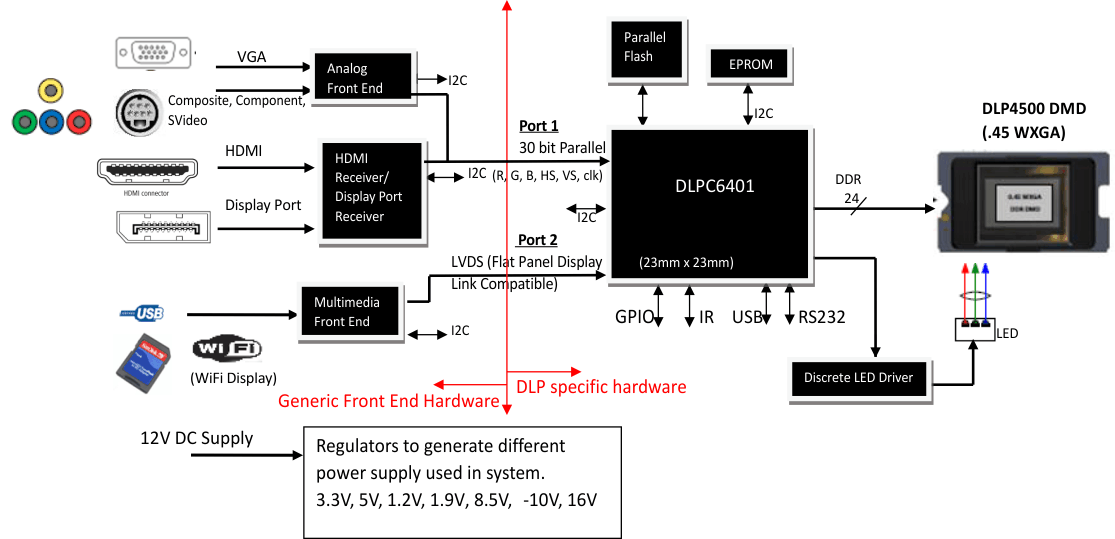
A common application when using the DLPC6401 is for creating a pico-projector that can be used as an accessory to a smartphone, tablet, or laptop. The DLPC6401 in the pico-projector receives images from a multimedia front-end within the product as shown in Figure 13.
 Figure 13. Typical Application Diagram
8.2.1 Design Requirements
A pico-projector is created by using a DLP chipset comprised of DLP4500 DMD and a DLPC6401 controller. The DLPC6401 controller does the digital image processing and the DLP4500 DMD is the display device for producing the projected image. In addition to the these DLP chips in the chipset, other chips may be needed. Typically a Flash part is needed to store the software and firmware. Additionally, a discrete LED driver solution is required to provide the LED driver functionality for LED illumination. The illumination light that is applied to the DMD is typically from red, green, and blue LEDs. These are often contained in three separate packages, but sometimes more than one color of LED die may be in the same package to reduce the overall size of the pico-projector. DLPC6401 controller provides either parallel- or LVDS-interface to connect the DLPC6401 controller to the multimedia front-end for receiving images and video.
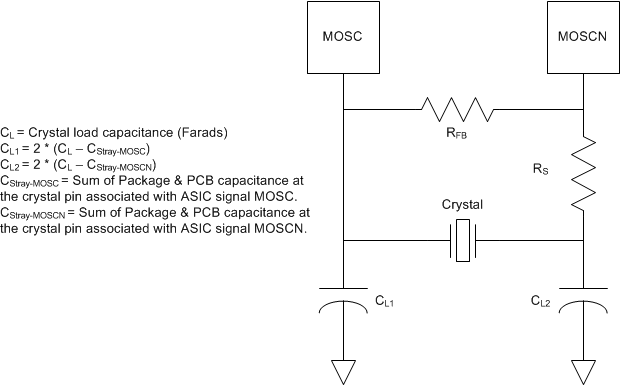
8.2.1.1 Recommended MOSC Crystal Oscillator Configuration
Table 8. Crystal Port Characteristics
| PARAMETER | NOMINAL | UNIT |
|---|---|---|
| MOSC to GND capacitance | 3.9 | pF |
| MOSCZ to GND capacitance | 3.8 | pF |
Table 9. Recommended Crystal Configuration(1)
| PARAMETER | RECOMMENDED | UNIT |
|---|---|---|
| Crystal circuit configuration | Parallel resonant | |
| Crystal type | Fundamental (first harmonic) | |
| Crystal nominal frequency | 32 | MHz |
| Crystal frequency temperature stability | ±30 | PPM |
| Overall crystal frequency tolerance (including accuracy, stability, aging, and trim sensitivity) | ±100 | PPM |
| Crystal ESR | 50 (max) | Ω |
| Crystal load | 10 | pF |
| Crystal shunt load | 7 (max) | pF |
| RS drive resistor (nominal) | 100 | Ω |
| RFB feedback resistor (nominal) | 1 | MΩ |
| CL1 external crystal load capacitor (MOSC) | See (1) | pF |
| CL2 external crystal load capacitor (MOSCN) | See (1) | pF |
| PCB layout | TI recommends a ground isolation ring around the crystal. |
 Figure 14. Recommended Crystal Oscillator Configuration
It is assumed that the external crystal oscillator will stabilize within 50 ms after stable power is applied.
8.2.2 Detailed Design Procedure
For connecting the DLPC6401 controller and the DLP4500 DMD together, see the reference design schematic. Layout guidelines should be followed to achieve a reliable projector. To complete the DLP system, an optical module or light engine is required that contains the DLP4500 DMD, associated illumination sources, optical elements, and necessary mechanical components.
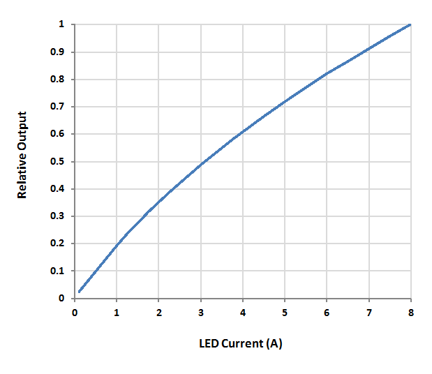
8.2.3 Application Curve
 Figure 15. Relative Output vs LED Current