ZHCSNH1C May 2021 – November 2022 DLPC6540
PRODUCTION DATA
- 1 特性
- 2 应用
- 3 说明
- 4 Revision History
- 5 Pin Configuration and Functions
-
6 Specifications
- 6.1 Absolute Maximum Ratings
- 6.2 ESD Ratings
- 6.3 Recommended Operating Conditions
- 6.4 Thermal Information
- 6.5 Power Electrical Characteristics
- 6.6 Pin Electrical Characteristics
- 6.7 DMD HSSI Electrical Characteristics
- 6.8 DMD Low-Speed LVDS Electrical Characteristics
- 6.9 V-by-One Interface Electrical Characteristics
- 6.10 USB Electrical Characteristics
- 6.11 System Oscillator Timing Requirements
- 6.12 Power Supply and Reset Timing Requirements
- 6.13 DMD HSSI Timing Requirements
- 6.14 DMD Low-Speed LVDS Timing Requirements
- 6.15 V-by-One Interface General Timing Requirements
- 6.16 Source Frame Timing Requirements
- 6.17 Synchronous Serial Port Interface Timing Requirements
- 6.18 Master and Slave I2C Interface Timing Requirements
- 6.19 Programmable Output Clock Timing Requirements
- 6.20 JTAG Boundary Scan Interface Timing Requirements (Debug Only)
- 6.21 JTAG ARM Multi-Ice Interface Timing Requirements (Debug Only)
- 6.22 Multi-Trace ETM Interface Timing Requirements
- 7 Detailed Description
- 8 Power Supply Recommendations
-
9 Layout
- 9.1
Layout Guidelines
- 9.1.1 General Layout Guidelines
- 9.1.2 Power Supply Layout Guidelines
- 9.1.3 Layout Guidelines for Internal Controller PLL Power
- 9.1.4 Layout Guideline for DLPC6540 Reference Clock
- 9.1.5 V-by-One Interface Layout Considerations
- 9.1.6 USB Interface Layout Considerations
- 9.1.7 DMD Interface Layout Considerations
- 9.1.8 General Handling Guidelines for Unused CMOS-Type Pins
- 9.1.9 Maximum Pin-to-Pin, PCB Interconnects Etch Lengths
- 9.2 Thermal Considerations
- 9.1
Layout Guidelines
- 10Device and Documentation Support
- 11Mechanical, Packaging, and Orderable Information
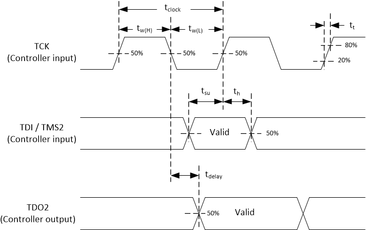
6.21 JTAG ARM Multi-Ice Interface Timing Requirements (Debug Only)
See Figure 6-19.
| PARAMETER | MIN | MAX | UNIT | ||
|---|---|---|---|---|---|
| ƒclock | Clock frequency, TCK | 8.33 | MHz | ||
| tclock | Clock period, TCK | 120 | ns | ||
| tw(H) | Pulse duration low, TCK | 50% reference points | 50 | ns | |
| tw(L) | Pulse duration high, TCK | 50% reference points | 50 | ns | |
| ts | Setup time – TDI valid before TCK↑ | 50% reference points | 15 | ns | |
| th | Hold time – TDI valid after TCK↑ | 50% reference points | 15 | ns | |
| ts | Setup time – TMS2 valid before TCK↑ | 50% reference points | 15 | ns | |
| th | Hold time – TMS2 valid after TCK↑ | 50% reference points | 15 | ns | |
| tt | Transition time (tr and tf) | 20% to 80% reference points | 5 | ns | |
| tdelay | Output delay, TCK↓ to TDO2 | 0 | 15 | ps | |
 Figure 6-19 Timing Diagram for JTAG ARM Multi-Ice