ZHCSNH1C May 2021 – November 2022 DLPC6540
PRODUCTION DATA
- 1 特性
- 2 应用
- 3 说明
- 4 Revision History
- 5 Pin Configuration and Functions
-
6 Specifications
- 6.1 Absolute Maximum Ratings
- 6.2 ESD Ratings
- 6.3 Recommended Operating Conditions
- 6.4 Thermal Information
- 6.5 Power Electrical Characteristics
- 6.6 Pin Electrical Characteristics
- 6.7 DMD HSSI Electrical Characteristics
- 6.8 DMD Low-Speed LVDS Electrical Characteristics
- 6.9 V-by-One Interface Electrical Characteristics
- 6.10 USB Electrical Characteristics
- 6.11 System Oscillator Timing Requirements
- 6.12 Power Supply and Reset Timing Requirements
- 6.13 DMD HSSI Timing Requirements
- 6.14 DMD Low-Speed LVDS Timing Requirements
- 6.15 V-by-One Interface General Timing Requirements
- 6.16 Source Frame Timing Requirements
- 6.17 Synchronous Serial Port Interface Timing Requirements
- 6.18 Master and Slave I2C Interface Timing Requirements
- 6.19 Programmable Output Clock Timing Requirements
- 6.20 JTAG Boundary Scan Interface Timing Requirements (Debug Only)
- 6.21 JTAG ARM Multi-Ice Interface Timing Requirements (Debug Only)
- 6.22 Multi-Trace ETM Interface Timing Requirements
- 7 Detailed Description
- 8 Power Supply Recommendations
-
9 Layout
- 9.1
Layout Guidelines
- 9.1.1 General Layout Guidelines
- 9.1.2 Power Supply Layout Guidelines
- 9.1.3 Layout Guidelines for Internal Controller PLL Power
- 9.1.4 Layout Guideline for DLPC6540 Reference Clock
- 9.1.5 V-by-One Interface Layout Considerations
- 9.1.6 USB Interface Layout Considerations
- 9.1.7 DMD Interface Layout Considerations
- 9.1.8 General Handling Guidelines for Unused CMOS-Type Pins
- 9.1.9 Maximum Pin-to-Pin, PCB Interconnects Etch Lengths
- 9.2 Thermal Considerations
- 9.1
Layout Guidelines
- 10Device and Documentation Support
- 11Mechanical, Packaging, and Orderable Information
7.3.5 Program Memory Flash Interface
The DLPC6540 provides three external program memory chip selects for devices to access the program memory interface. These are detailed in Table 7-16.
Table 7-16 Program Memory Interface Chip
Selects
| CHIP SELECT NAME | CHIP SELECT USE | DATA BUS WIDTH | ACCESS TIME | MAXIMUM SIZE SUPPORTED (1) |
|---|---|---|---|---|
| PM_CSZ_0 | Boot FLASH only - Required (2) | 16 bits | < = 120ns | 256Mb |
| PM_CSZ_1 | Additional Peripheral Device (or additional FLASH) - Optional | 16 bits | < = 120ns | 256Mb |
| PM_CSZ_2 | Additional Peripheral Device - Optional | 16 bits | < = 120ns | 256Mb |
(1) Using GPIO_47 as additional address bit
(2) Boot FLASH type supported is Standard NOR parallel FLASH,
single or multi-bank.
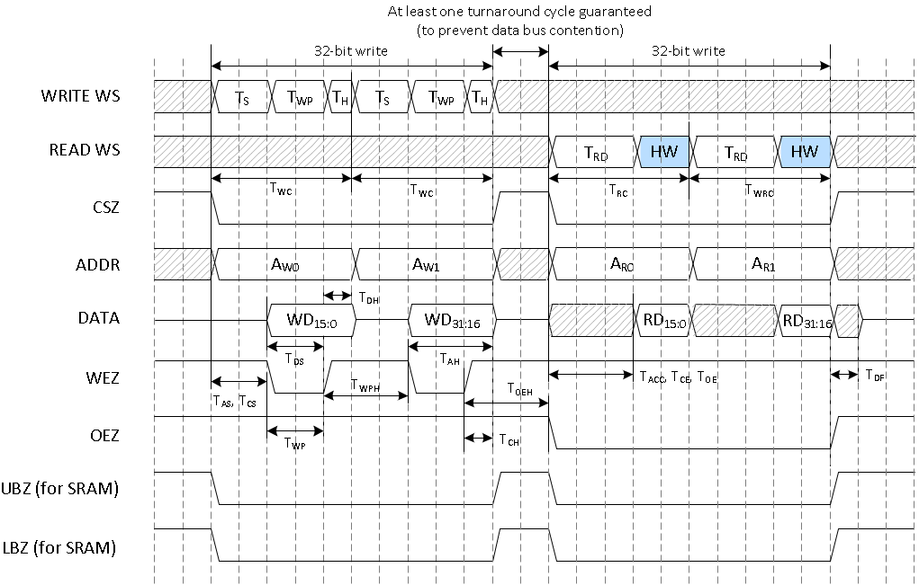
FLASH access timing is software programmable with up to 31 wait states. Additional information about read and write wait state timing is provided in Table 7-17 and Figure 7-1.
Table 7-17 Program Memory Wait State
Timing
| PARAMETER | EQUATION (1) |
|---|---|
| TWSR: Wait State Resolution | 6ns |
| Read Wait States (Number of Read Wait States for each CSz read access) |
ROUNDUP(MAX(TACC, TCE,TOE)/TWSR-N) (2)(3) |
| Write Wait States for TCSand
TAS (Time from CS/Address activation to WRZ assertion) |
ROUNDUP(MAX(TCS+5ns, TAS+5ns)/TWSR-N) (2) |
| Write Wait States for TWP and
TDS (Time from WRZ assertion to WEZ de-assertion) |
ROUNDUP(MAX(TWP+5ns, TDS+5ns)/TWSR-N) (2) |
| Write Wait States for TCHand
TDH (Time from CS/Address activation to WRZ assertion) |
ROUNDUP(MAX(TCH+5ns, TDH+5ns)/TWSR-N) (2) |
(1)
- TACC: Read Access Time (ADDR to DATA valid) – (address valid to DATA valid)
- TCE: Read Access Time (CSZ to DATA valid) – (chip select active to DATA valid)
- TOE: Read Access Time (OEZ to DATA valid) – (output enable active to DATA valid)
- TCS: CSZ Setup Time (Writes) – (chip select active before negedge(WEZ)
- TCS: Address Setup Time (Writes) – (address valid before negedge(WEZ)
- TAS: Address Setup Time (Writes) – (address valid before negedge(WEZ)
- TWP: Write Pulse Width (Writes) – (WEZ active low time)
- TDS: Data Setup Time (Writes) – (DATA valid before posedge(WEZ)
- TCH: CSZ Hold Time (Writes) – (CSZ held active after posedge(WEZ)
- TDH: Data Hold Time (Writes) – (DATA held valid after posedge(WEZ)
(2) Requires a minimum of at least 1 wait state
(3) Assumes a maximum single direction trace length of 90 mm (3.5
inches)
 Figure 7-1 Program
Memory Interface Timing Diagram