ZHCSNH1C May 2021 – November 2022 DLPC6540
PRODUCTION DATA
- 1 特性
- 2 应用
- 3 说明
- 4 Revision History
- 5 Pin Configuration and Functions
-
6 Specifications
- 6.1 Absolute Maximum Ratings
- 6.2 ESD Ratings
- 6.3 Recommended Operating Conditions
- 6.4 Thermal Information
- 6.5 Power Electrical Characteristics
- 6.6 Pin Electrical Characteristics
- 6.7 DMD HSSI Electrical Characteristics
- 6.8 DMD Low-Speed LVDS Electrical Characteristics
- 6.9 V-by-One Interface Electrical Characteristics
- 6.10 USB Electrical Characteristics
- 6.11 System Oscillator Timing Requirements
- 6.12 Power Supply and Reset Timing Requirements
- 6.13 DMD HSSI Timing Requirements
- 6.14 DMD Low-Speed LVDS Timing Requirements
- 6.15 V-by-One Interface General Timing Requirements
- 6.16 Source Frame Timing Requirements
- 6.17 Synchronous Serial Port Interface Timing Requirements
- 6.18 Master and Slave I2C Interface Timing Requirements
- 6.19 Programmable Output Clock Timing Requirements
- 6.20 JTAG Boundary Scan Interface Timing Requirements (Debug Only)
- 6.21 JTAG ARM Multi-Ice Interface Timing Requirements (Debug Only)
- 6.22 Multi-Trace ETM Interface Timing Requirements
- 7 Detailed Description
- 8 Power Supply Recommendations
-
9 Layout
- 9.1
Layout Guidelines
- 9.1.1 General Layout Guidelines
- 9.1.2 Power Supply Layout Guidelines
- 9.1.3 Layout Guidelines for Internal Controller PLL Power
- 9.1.4 Layout Guideline for DLPC6540 Reference Clock
- 9.1.5 V-by-One Interface Layout Considerations
- 9.1.6 USB Interface Layout Considerations
- 9.1.7 DMD Interface Layout Considerations
- 9.1.8 General Handling Guidelines for Unused CMOS-Type Pins
- 9.1.9 Maximum Pin-to-Pin, PCB Interconnects Etch Lengths
- 9.2 Thermal Considerations
- 9.1
Layout Guidelines
- 10Device and Documentation Support
- 11Mechanical, Packaging, and Orderable Information
6.13 DMD HSSI Timing Requirements
over operating free-air temperature range (unless otherwise noted)
| PARAMETER | MIN | NOM | MAX | UNIT | ||
|---|---|---|---|---|---|---|
| Baud | Baud Rate | 2.4 | 3.2 | Gbps | ||
| UI | Unit Interval, 1/Baud | 312.5 | 416.7 | ps | ||
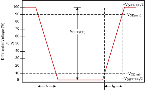
| tR | Differential output rise time (1)(2) (0% to 100% of minimum eye mask height) |
Data | 50 | 115 | ps | |
| Clock | 50 | 135 | ps | |||
| tF | Differential output fall time(1)(2) (0% to 100% of minimum eye mask height) |
Data | 50 | 115 | ps | |
| Clock | 50 | 135 | ps | |||
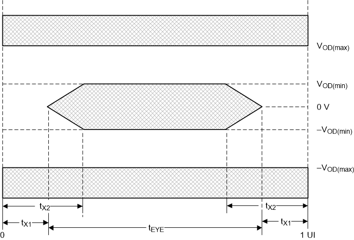
| tX1 | Maximum eye closure(3) | at zero crossing | 0.15 | UI | ||
| tX2 | Maximum eye closure(3) | at minimum eye height | 0.375 | UI | ||
| tEYE | Differential Data Eye(3) | 0.7 | UI | |||
| tskln2ln | Lane to lane skew within a macro(2) | |200| | ps | |||
| tskM2M | Lane to lane skew macro to macro(2) | |4UI+200| | ps | |||
| fSSCD | Spread Spectrum (down spreading only) (4) | When SSCD Enabled | 1 | % | ||
| fMOD | Modulation Frequency (4) | When SSCD Enabled | 78.125 | KHz | ||
(1) Rise and
fall
times are associated with VDIFF-pp as shown in Figure 6-10.
(2) Measured with an interconnect
with an insertion loss of 3dB at 1.6 GHz
(3) See Figure 6-11
(4) When SSCD is enabled, the available modulation waveform is: Triangular

VCM is removed when
signals are viewed differentially.
Figure 6-10 HSSI Differential Timing Parameters Figure 6-11 HSSI Eye
Characteristics