ZHCSNH1C May 2021 – November 2022 DLPC6540
PRODUCTION DATA
- 1 特性
- 2 应用
- 3 说明
- 4 Revision History
- 5 Pin Configuration and Functions
-
6 Specifications
- 6.1 Absolute Maximum Ratings
- 6.2 ESD Ratings
- 6.3 Recommended Operating Conditions
- 6.4 Thermal Information
- 6.5 Power Electrical Characteristics
- 6.6 Pin Electrical Characteristics
- 6.7 DMD HSSI Electrical Characteristics
- 6.8 DMD Low-Speed LVDS Electrical Characteristics
- 6.9 V-by-One Interface Electrical Characteristics
- 6.10 USB Electrical Characteristics
- 6.11 System Oscillator Timing Requirements
- 6.12 Power Supply and Reset Timing Requirements
- 6.13 DMD HSSI Timing Requirements
- 6.14 DMD Low-Speed LVDS Timing Requirements
- 6.15 V-by-One Interface General Timing Requirements
- 6.16 Source Frame Timing Requirements
- 6.17 Synchronous Serial Port Interface Timing Requirements
- 6.18 Master and Slave I2C Interface Timing Requirements
- 6.19 Programmable Output Clock Timing Requirements
- 6.20 JTAG Boundary Scan Interface Timing Requirements (Debug Only)
- 6.21 JTAG ARM Multi-Ice Interface Timing Requirements (Debug Only)
- 6.22 Multi-Trace ETM Interface Timing Requirements
- 7 Detailed Description
- 8 Power Supply Recommendations
-
9 Layout
- 9.1
Layout Guidelines
- 9.1.1 General Layout Guidelines
- 9.1.2 Power Supply Layout Guidelines
- 9.1.3 Layout Guidelines for Internal Controller PLL Power
- 9.1.4 Layout Guideline for DLPC6540 Reference Clock
- 9.1.5 V-by-One Interface Layout Considerations
- 9.1.6 USB Interface Layout Considerations
- 9.1.7 DMD Interface Layout Considerations
- 9.1.8 General Handling Guidelines for Unused CMOS-Type Pins
- 9.1.9 Maximum Pin-to-Pin, PCB Interconnects Etch Lengths
- 9.2 Thermal Considerations
- 9.1
Layout Guidelines
- 10Device and Documentation Support
- 11Mechanical, Packaging, and Orderable Information
9.1.6 USB Interface Layout Considerations
The DLPC6540 USB differential interface waveform quality and timing is dependent on the total length of the interconnect system, the spacing between traces, the characteristic impedance, etch losses, and how well matched the lengths are across the interface. Thus, ensuring positive timing margin requires attention to many factors.
DLPC6540 I/O timing parameters, USB transmitter and receiver timing parameters, as well as USB specific timing requirements can be found in their corresponding data sheets. PCB routing mismatch can be budgeted and met through controlled PCB routing. PCB related requirements for USB are provided in Table 9-6 as a starting point for the customer.
| PARAMETER | MIN | TYP | MAX | UNIT |
|---|---|---|---|---|
| Cross-talk between data lane (USB_DAT_P, USB_DAT_N) and other signals | < 1.5 | mVpp | ||
| Intra-lane skew (USB_DAT_P, USB_DAT_N) | < 20 | ps | ||
| Differential Impedance (USB_DAT_P, USB_DAT_N) | 76.5 | 90 | 103.5 | Ω |
| Single Mode impedance (USB_DAT_P, USB_DAT_N) | 45 | Ω | ||
| Common Mode Impedance (USB_DAT_P, USB_DAT_N) | 21 | 30 | 39 | Ω |
| Parasitic resistance (USB_DAT_P, USB_DAT_N) | ≤ 0.5 | Ω | ||
| Total capacitance (USB_DAT_P, USB_DAT_N) | < 4 | pF | ||
| Differences of trace capacitance between USB_DAT_P, USB_DAT_N | < 1 | pF | ||
| TXRTUNE resistor | 172.26 | 174 | 175.74 | Ω |
Additional layout guidelines for USB_DAT_P/USB_DAT_N:
- Route the differential signal pairs on the top layer of the PBC to minimize the number of vias. Limit the number of necessary vias to two.
- Route differential signal pairs over a single ground or power plane using a Micro-strip line configuration. Ground guard traces are also recommended.
- Do not route the differential signal pairs over the slit of power or ground planes.
- Minimize the trace length mismatch for each pair, and between each pair, in order to meet the skew requirements.
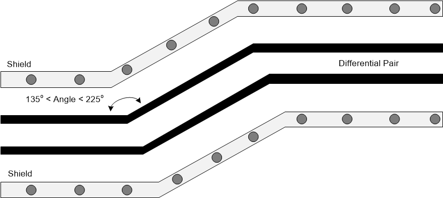
- Ensure that the bend angles associated with the differential signal pair are between 135o and 225o. (See Figure 9-14).
- Minimize the length where the differential signal pair are parallel to clocks or digital signals.
- Do not route the differential signal pair under an IC that uses a quartz crystal, oscillator, clock synchronization circuit, magnetic device, or clock.
 Figure 9-13 USB Layout Example
 Figure 9-14 USB Routing Example
Additional USB layout guidelines for TXRTUNE
- Use the shortest possible connection lengths for the resistor between TXRTUNE and ground.
- Use ground layer and ground guard traces to shield the wires and resistor.