ZHCSD20H October 2014 – June 2024 DLPC900
PRODUCTION DATA
- 1
- 1 特性
- 2 应用
- 3 说明
- 4 Pin Configuration and Functions
-
5 Specifications
- 5.1 Absolute Maximum Ratings
- 5.2 ESD Ratings
- 5.3 Recommended Operating Conditions
- 5.4 Thermal Information
- 5.5 Electrical Characteristics
- 5.6 System Oscillators Timing Requirements #GUID-909D0FD3-84C7-4481-924A-4FDE7EB548A1/DLPS0373944
- 5.7 Power-Up and Power-Down Timing Requirements
- 5.8 JTAG Interface: I/O Boundary Scan Application Timing Requirements
- 5.9 JTAG Interface: I/O Boundary Scan Application Switching Characteristics
- 5.10 Programmable Output Clocks Switching Characteristics
- 5.11 Port 1 and 2 Input Pixel Interface Timing Requirements
- 5.12 Two Pixels Per Clock (48-Bit Bus) Timing Requirements
- 5.13 Synchronous Serial Port (SSP) Switching Characteristics
- 5.14 DMD Interface Switching Characteristics
- 5.15 DMD LVDS Interface Switching Characteristics
- 5.16 Source Input Blanking Requirements
-
6 Detailed Description
- 6.1 Overview
- 6.2 Functional Block Diagram
- 6.3
Feature Description
- 6.3.1 DMD Configurations
- 6.3.2 Video Timing Input Blanking Specification
- 6.3.3 Board-Level Test Support
- 6.3.4 Two Controller Considerations
- 6.3.5 Memory Design Considerations
- 6.4 Device Functional Modes
-
7 Application and Implementation
- 7.1 Application Information
- 7.2
Typical Applications
- 7.2.1 Typical Two Controller Chipset
- 7.2.2 Typical Single Controller Chipset
- 8 Power Supply Recommendations
-
9 Layout
- 9.1
Layout Guidelines
- 9.1.1 General PCB Recommendations
- 9.1.2 PCB Layout Guidelines for Internal Controller PLL Power
- 9.1.3 PCB Layout Guidelines for Quality Video Performance
- 9.1.4 Recommended MOSC Crystal Oscillator Configuration
- 9.1.5 Spread Spectrum Clock Generator Support
- 9.1.6 GPIO Interface
- 9.1.7 General Handling Guidelines for Unused CMOS-Type Pins
- 9.1.8 DMD Interface Considerations
- 9.1.9 PCB Design Standards
- 9.1.10 Signal Layers
- 9.1.11 Trace Widths and Minimum Spacing
- 9.1.12 Trace Impedance and Routing Priority
- 9.1.13 Power and Ground Planes
- 9.1.14 Power Vias
- 9.1.15 Decoupling
- 9.1.16 Fiducials
- 9.2 Layout Example
- 9.3 Thermal Considerations
- 9.1
Layout Guidelines
- 10Device and Documentation Support
- 11Revision History
- 12Mechanical, Packaging, and Orderable Information
6.3 Feature Description
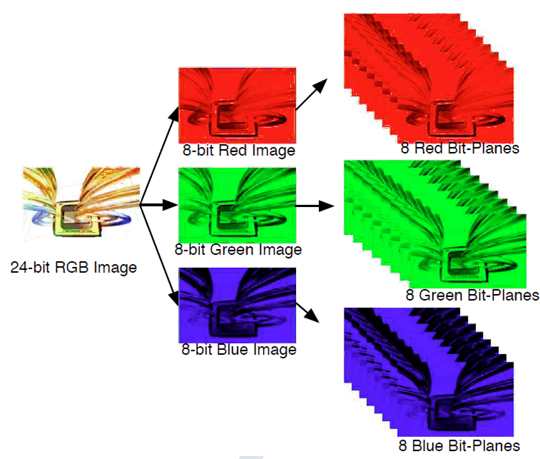
The DLPC900 controller takes as input 16-, 20-, or 24-bit RGB data at up to 120Hz frame rate. For example, a 120Hz 24-bit frame is composed of three colors (red, green, and blue) with each color equally divided in the 120Hz frame rate. Thus, each color has a 2.78ms time slot allocated. Because each color has an 8-bit depth, each color time slot is further divided into bit-planes. A bit-plane is the 2-dimensional arrangement of one-bit extracted from all the pixels in the full-color 2D image to implement dynamic depth (see Figure 6-2).
 Figure 6-2 Bit Slices
The length of each bit-plane in the time slot is weighted by the corresponding power of two of its binary representations. This provides a binary pulse-width modulation of the image. For example, a 24-bit RGB input has three colors (R, G, and B) with 8-bit depth each. Each color time slot is then divided into eight bit-planes, with the sum of the weight of all bit planes in the time slot equal to 256. Figure 6-3 illustrates the time partition of the bits in one 8-bit color time slot within a 24-bit RGB frame.
 Figure 6-3 24-Bit RGB Frame Bit Partition
Therefore, a single video frame is composed of a series of bit-planes. Because the DMD mirrors can be either on or off, an image is created by turning on the mirrors corresponding to the bit set in a bit-plane. With binary pulse-width modulation, the intensity level of the color is reproduced by controlling the amount of time the mirror is on. For a 24-bit RGB frame image inputted to the DLPC900 controller, the DLPC900 controller creates 24 bit-planes, stores them in internal embedded DRAM, and sends them to the DMD, one bit-plane at a time. The bit weight controls the amount of time the mirror is on. To improve image quality in video frames, these bit-planes, time slots, and color frames are shuffled and interleaved within the pixel processing functions of the DLPC900 controller.