ZHCSD20H October 2014 – June 2024 DLPC900
PRODUCTION DATA
- 1
- 1 特性
- 2 应用
- 3 说明
- 4 Pin Configuration and Functions
-
5 Specifications
- 5.1 Absolute Maximum Ratings
- 5.2 ESD Ratings
- 5.3 Recommended Operating Conditions
- 5.4 Thermal Information
- 5.5 Electrical Characteristics
- 5.6 System Oscillators Timing Requirements #GUID-909D0FD3-84C7-4481-924A-4FDE7EB548A1/DLPS0373944
- 5.7 Power-Up and Power-Down Timing Requirements
- 5.8 JTAG Interface: I/O Boundary Scan Application Timing Requirements
- 5.9 JTAG Interface: I/O Boundary Scan Application Switching Characteristics
- 5.10 Programmable Output Clocks Switching Characteristics
- 5.11 Port 1 and 2 Input Pixel Interface Timing Requirements
- 5.12 Two Pixels Per Clock (48-Bit Bus) Timing Requirements
- 5.13 Synchronous Serial Port (SSP) Switching Characteristics
- 5.14 DMD Interface Switching Characteristics
- 5.15 DMD LVDS Interface Switching Characteristics
- 5.16 Source Input Blanking Requirements
-
6 Detailed Description
- 6.1 Overview
- 6.2 Functional Block Diagram
- 6.3
Feature Description
- 6.3.1 DMD Configurations
- 6.3.2 Video Timing Input Blanking Specification
- 6.3.3 Board-Level Test Support
- 6.3.4 Two Controller Considerations
- 6.3.5 Memory Design Considerations
- 6.4 Device Functional Modes
-
7 Application and Implementation
- 7.1 Application Information
- 7.2
Typical Applications
- 7.2.1 Typical Two Controller Chipset
- 7.2.2 Typical Single Controller Chipset
- 8 Power Supply Recommendations
-
9 Layout
- 9.1
Layout Guidelines
- 9.1.1 General PCB Recommendations
- 9.1.2 PCB Layout Guidelines for Internal Controller PLL Power
- 9.1.3 PCB Layout Guidelines for Quality Video Performance
- 9.1.4 Recommended MOSC Crystal Oscillator Configuration
- 9.1.5 Spread Spectrum Clock Generator Support
- 9.1.6 GPIO Interface
- 9.1.7 General Handling Guidelines for Unused CMOS-Type Pins
- 9.1.8 DMD Interface Considerations
- 9.1.9 PCB Design Standards
- 9.1.10 Signal Layers
- 9.1.11 Trace Widths and Minimum Spacing
- 9.1.12 Trace Impedance and Routing Priority
- 9.1.13 Power and Ground Planes
- 9.1.14 Power Vias
- 9.1.15 Decoupling
- 9.1.16 Fiducials
- 9.2 Layout Example
- 9.3 Thermal Considerations
- 9.1
Layout Guidelines
- 10Device and Documentation Support
- 11Revision History
- 12Mechanical, Packaging, and Orderable Information
9.1.2 PCB Layout Guidelines for Internal Controller PLL Power
The following are guidelines to achieve desired controller performance relative to internal PLLs:
The DLPC900 contains four PLLs (PLLM1, PLLM2, PLLD, and PLLS), each of which have a dedicated 1.15V digital supply; three of these PLLs (PLLM1, PLLM2, and PLLD) have a dedicated 1.8V analog supply. It is important to have filtering on the supply pins that covers a broad frequency range. Each 1.15V PLL supply pin must have individual high frequency filtering in the form of a ferrite bead and a 0.1µF ceramic capacitor. These components must be located very close to the individual PLL supply balls. The impedance of the ferrite bead should far exceed that of the capacitor at frequencies above 10MHz. The 1.15V to the PLL supply pins must also have low frequency filtering in the form of an RC filter. This filter can be common to all the PLLs. The voltage drop across the resistor is limited by the 1.15V regulator tolerance and the DLPC900 voltage tolerance. A resistance of 0.36Ω and a 100µF ceramic are recommended. Figure 9-1 shows the recommended filter topology.
 Figure 9-1 Recommended Filter
Topology for PLL 1.15V Supplies
Figure 9-1 Recommended Filter
Topology for PLL 1.15V SuppliesThe analog 1.8V PLL power pins must have a similar filter topology as the 1.15V. In addition, it is recommended that a dedicated linear regulator generates the 1.8V. Figure 9-2 shows the recommended filtering topology.
 Figure 9-2 Recommended Filter
Topology for PLL 1.8V Supplies
Figure 9-2 Recommended Filter
Topology for PLL 1.8V SuppliesWhen designing the overall supply filter network, care must be taken to ensure no resonance occurs. Specific care is required around the 1MHz to 2MHz band, as this coincides with the PLL natural loop frequency.
 Figure 9-3 High Frequency Decoupling
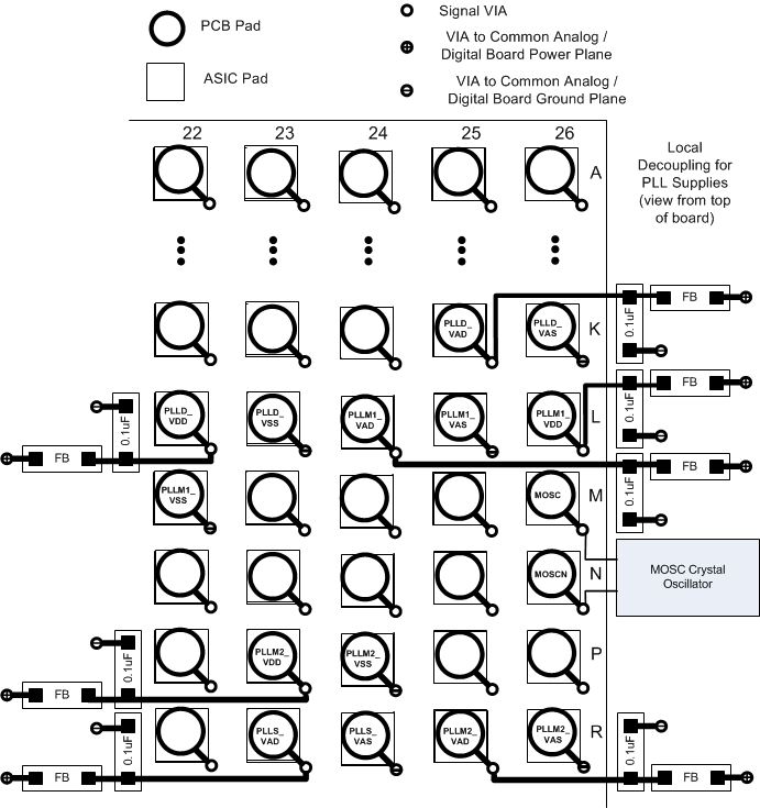
High-frequency decoupling is required for 1.15V and 1.8V PLL supplies and must be provided as close as possible to each of the PLL supply package pins as shown in Figure 9-3. Placing decoupling capacitors under the package on the opposite side of the board is recommended. High-quality, low-ESR, monolithic, surface-mount capacitors are recommended for use. Typically, 0.1µF for each PLL supply should be sufficient. The length of a connecting trace increases the parasitic inductance of the mounting, and thus, where possible, there can be no trace, allowing the via to butt up against the land. Additionally, the connecting trace must be made as wide as possible. Further improvement can be made by placing vias to the side of the capacitor lands or doubling the number of vias.
The location of bulk decoupling depends on the system design.