ZHCSE90D September   2015  – September 2020 DLPC910

PRODUCTION DATA  

  1. 特性
  2. 应用
  3. 说明
  4. Revision History
  5. Pin Configuration and Functions
    1.     Pin Functions
  6. Specifications
    1. 6.1 Absolute Maximum Ratings
    2. 6.2 ESD Ratings
    3. 6.3 Recommended Operating Conditions
    4. 6.4 Thermal Information
    5. 6.5 Electrical Characteristics
    6. 6.6 Timing Requirements
  7. Detailed Description
    1. 7.1 Overview
    2. 7.2 Functional Block Diagram
    3. 7.3 Feature Description
      1. 7.3.1  Input LVDS Interface
      2. 7.3.2  Data Clock
      3. 7.3.3  Data Valid
      4. 7.3.4  Interface Training
      5. 7.3.5  Row and Block Interface
        1. 7.3.5.1 Row Mode
        2. 7.3.5.2 Block Mode
      6. 7.3.6  Control Interface
        1. 7.3.6.1 Complement Data
        2. 7.3.6.2 North South Flip
        3. 7.3.6.3 Watchdog
        4. 7.3.6.4 DMD Mirror Float
        5. 7.3.6.5 Load4
          1. 7.3.6.5.1 Load4 Row Addressing
          2. 7.3.6.5.2 Load4 Block Clears
      7. 7.3.7  Status Interface
        1. 7.3.7.1 ECP2 Finished
        2. 7.3.7.2 Initialization Active
        3. 7.3.7.3 Reset Active
        4. 7.3.7.4 DMD_TYPE
        5. 7.3.7.5 DDC_Version(2:0)
        6. 7.3.7.6 DMD_IRQ
        7. 7.3.7.7 LED Indicators
          1. 7.3.7.7.1 VLED0
          2. 7.3.7.7.2 VLED1
      8. 7.3.8  Reset and System Clock
        1. 7.3.8.1 Controller Reset
        2. 7.3.8.2 Main Oscillator Clock
      9. 7.3.9  I2C Interface
        1. 7.3.9.1 Configuration Pins
        2. 7.3.9.2 Communications Interface
          1. 7.3.9.2.1 Command Format
      10. 7.3.10 DMD Interface
        1. 7.3.10.1 DDC_DOUT
        2. 7.3.10.2 DDC_SCTRL
        3. 7.3.10.3 DDC_DCLKOUT
        4. 7.3.10.4 DMD Reset Interface
          1. 7.3.10.4.1 Mirror Reset Control
        5. 7.3.10.5 Enable and Interrupt Signals
        6. 7.3.10.6 Serial Control Port
      11. 7.3.11 Flash PROM Interface
        1. 7.3.11.1 JTAG Interface
        2. 7.3.11.2 PGM Interface
    4. 7.4 Device Functional Modes
      1. 7.4.1 DMD Row Operation
        1. 7.4.1.1 Data and Command Write Cycle
      2. 7.4.2 Block Mode Operation
      3. 7.4.3 Block Clear
      4. 7.4.4 Mirror Clocking Pulse
      5. 7.4.5 DMD Array Subset
      6. 7.4.6 Global Mirror Clocking Pulse Consideration
    5. 7.5 Register Map
      1. 7.5.1 Register Table Overview
        1. 7.5.1.1  DESTOP_INTERRUPT Register
        2. 7.5.1.2  MAIN_STATUS Register
        3. 7.5.1.3  DESTOP_CAL Register
        4. 7.5.1.4  DESTOP_DMD_ID_REG Register
        5. 7.5.1.5  DESTOP_CATBITS_REG Register
        6. 7.5.1.6  DESTOP_VERSION Register
        7. 7.5.1.7  DESTOP_RESET_REG Register
        8. 7.5.1.8  DESTOP_INFIFO_STATUS Register
        9. 7.5.1.9  DESTOP_BUS_SWAP Register
        10. 7.5.1.10 DESTOP_DMDCTRL Register
        11. 7.5.1.11 DESTOP_BIT_FLIP Register
  8. Application and Implementation
    1. 8.1 Application Information
    2. 8.2 Typical Application
      1. 8.2.1 High Speed Lithography Application
        1. 8.2.1.1 Design Requirements
        2. 8.2.1.2 Detailed Design Procedure
        3. 8.2.1.3 Application Curves
  9. Power Supply Recommendations
    1. 9.1 Power Supply Distribution and Requirements
    2. 9.2 Power Down Requirements
  10. 10Layout
    1. 10.1 Layout Guidelines
      1. 10.1.1 PCB Design Standards
      2. 10.1.2 Signal Layers
      3. 10.1.3 General PCB Routing
        1. 10.1.3.1 Trace Minimum Spacing
        2. 10.1.3.2 Trace Widths and Lengths
          1. 10.1.3.2.1 LVDS Output Bus Skew
        3. 10.1.3.3 Trace Impedance and Routing Priority
      4. 10.1.4 Power and Ground Planes
      5. 10.1.5 Power Vias
      6. 10.1.6 Decoupling
      7. 10.1.7 Flex Connector Plating
    2. 10.2 Layout Example
  11. 11Device and Documentation Support
    1. 11.1 Device Support
      1. 11.1.1 Device Nomenclature
      2. 11.1.2 Device Markings
    2. 11.2 Documentation Support
      1. 11.2.1 Related Documentation
    3. 11.3 支持资源
    4. 11.4 Trademarks
    5. 11.5 静电放电警告
    6. 11.6 术语表
  12. 12Mechanical, Packaging, and Orderable Information

封装选项

机械数据 (封装 | 引脚)
散热焊盘机械数据 (封装 | 引脚)
订购信息

Timing Requirements

(see (1))
MINNOMMAXUNIT
fcdClock frequency, DCLKIN_n (2)400MHz
480
fcrClock frequency, CLK_R50MHz
tcCycle time, DCLKIN_nfcd = 400 MHz2.5ns
fcd = 480 MHz2.083
tw(H)Pulse duration, high50% to 50% reference points (signal)fcd = 400 MHz1.25ns
fcd = 480 MHz1.042
tw(L)Pulse duration, low50% to 50% reference points (signal)fcd = 400 MHz1.25ns
fcd = 480 MHz1.042
ttTransition time, tt = tf /tr20% to 80% reference points (signal)fcd = 400 MHz0.6ns
fcd = 480 MHz0.5
tjpPeriod Jitter DCLKIN_n (3)100ps
tskSkew, DIN_A(15-0) to DCLKIN_A-100100ps
Skew, DIN_B(15-0) to DCLKIN_B-100100
Skew, DIN_C(15-0) to DCLKIN_C-100100
Skew, DIN_D(15-0) to DCLKIN_D-100100
Skew, DVALID_n to DCLKIN_n↑-100100
Skew, BLKMD BLKAD to DCLKIN_n↑ (4)-100100
Skew, ROWMD or ROWAD to DCLKIN_n↑ (4)-100100
Skew, STEPVCC to DCLKIN↑ (4)-100100
It is recommended that the COMP_DATA, NS_FLIP and RST2BLK flags be set to one value and not adjusted during normal system operation.
Preferred DDC_DCLK _n duty cycle = 50%
This is the deviation in period from ideal period due solely to high frequency jitter.
First edge of DDC_DIN*, ROW*, and BLK* should be synchronous to DVALID rising edge.
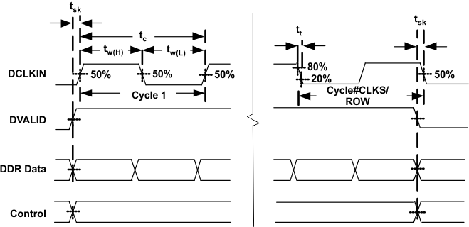
GUID-FB0DD27F-2E80-440B-8ED6-F99A76620127-low.gifFigure 6-1 Input Interface Timing
Note: Dynamic changes to RST2BLK, NS_FLIP and COMP_DATA during normal operation are not recommended.