ZHCSE90D September 2015 – September 2020 DLPC910
PRODUCTION DATA
- 1 特性
- 2 应用
- 3 说明
- 4 Revision History
- 5 Pin Configuration and Functions
- 6 Specifications
-
7 Detailed Description
- 7.1 Overview
- 7.2 Functional Block Diagram
- 7.3 Feature Description
- 7.4 Device Functional Modes
- 7.5
Register Map
- 7.5.1
Register Table Overview
- 7.5.1.1 DESTOP_INTERRUPT Register
- 7.5.1.2 MAIN_STATUS Register
- 7.5.1.3 DESTOP_CAL Register
- 7.5.1.4 DESTOP_DMD_ID_REG Register
- 7.5.1.5 DESTOP_CATBITS_REG Register
- 7.5.1.6 DESTOP_VERSION Register
- 7.5.1.7 DESTOP_RESET_REG Register
- 7.5.1.8 DESTOP_INFIFO_STATUS Register
- 7.5.1.9 DESTOP_BUS_SWAP Register
- 7.5.1.10 DESTOP_DMDCTRL Register
- 7.5.1.11 DESTOP_BIT_FLIP Register
- 7.5.1
Register Table Overview
- 8 Application and Implementation
- 9 Power Supply Recommendations
- 10Layout
- 11Device and Documentation Support
- 12Mechanical, Packaging, and Orderable Information
10.2 Layout Example
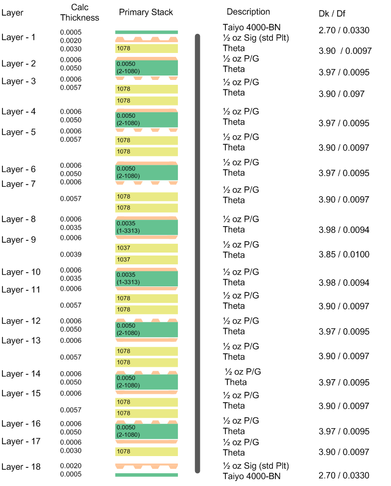
The PCB layer design may vary depending on system design. However, careful attention is required to meet design considerations. Table 10-7 shows a layer signal definition and Figure 10-1 shows a PCB stack-up. The PCB stack-up uses Hitachi 679gs as the dielectric material to improve the signal slew rate. Although the material shown is Rogers Theta, it is the same material as the Hitachi 679gs.
Table 10-7 Layer Definition
| Top: | Signal |
|---|---|
| 2: | GND |
| 3: | Signal |
| 4: | GND |
| 5: | Signal |
| 6: | GND |
| 7: | Signal |
| 8: | GND |
| 9: | Split Power |
| 10: | Split Power |
| 11: | GND |
| 12: | Signal |
| 13: | GND |
| 14: | Signal |
| 15: | GND |
| 16: | Signal |
| 17: | GND |
| Bottom: | Signal |
 Figure 10-1 PCB Stack-Up