ZHCSE90D September   2015  – September 2020 DLPC910

PRODUCTION DATA  

  1. 特性
  2. 应用
  3. 说明
  4. Revision History
  5. Pin Configuration and Functions
    1.     Pin Functions
  6. Specifications
    1. 6.1 Absolute Maximum Ratings
    2. 6.2 ESD Ratings
    3. 6.3 Recommended Operating Conditions
    4. 6.4 Thermal Information
    5. 6.5 Electrical Characteristics
    6. 6.6 Timing Requirements
  7. Detailed Description
    1. 7.1 Overview
    2. 7.2 Functional Block Diagram
    3. 7.3 Feature Description
      1. 7.3.1  Input LVDS Interface
      2. 7.3.2  Data Clock
      3. 7.3.3  Data Valid
      4. 7.3.4  Interface Training
      5. 7.3.5  Row and Block Interface
        1. 7.3.5.1 Row Mode
        2. 7.3.5.2 Block Mode
      6. 7.3.6  Control Interface
        1. 7.3.6.1 Complement Data
        2. 7.3.6.2 North South Flip
        3. 7.3.6.3 Watchdog
        4. 7.3.6.4 DMD Mirror Float
        5. 7.3.6.5 Load4
          1. 7.3.6.5.1 Load4 Row Addressing
          2. 7.3.6.5.2 Load4 Block Clears
      7. 7.3.7  Status Interface
        1. 7.3.7.1 ECP2 Finished
        2. 7.3.7.2 Initialization Active
        3. 7.3.7.3 Reset Active
        4. 7.3.7.4 DMD_TYPE
        5. 7.3.7.5 DDC_Version(2:0)
        6. 7.3.7.6 DMD_IRQ
        7. 7.3.7.7 LED Indicators
          1. 7.3.7.7.1 VLED0
          2. 7.3.7.7.2 VLED1
      8. 7.3.8  Reset and System Clock
        1. 7.3.8.1 Controller Reset
        2. 7.3.8.2 Main Oscillator Clock
      9. 7.3.9  I2C Interface
        1. 7.3.9.1 Configuration Pins
        2. 7.3.9.2 Communications Interface
          1. 7.3.9.2.1 Command Format
      10. 7.3.10 DMD Interface
        1. 7.3.10.1 DDC_DOUT
        2. 7.3.10.2 DDC_SCTRL
        3. 7.3.10.3 DDC_DCLKOUT
        4. 7.3.10.4 DMD Reset Interface
          1. 7.3.10.4.1 Mirror Reset Control
        5. 7.3.10.5 Enable and Interrupt Signals
        6. 7.3.10.6 Serial Control Port
      11. 7.3.11 Flash PROM Interface
        1. 7.3.11.1 JTAG Interface
        2. 7.3.11.2 PGM Interface
    4. 7.4 Device Functional Modes
      1. 7.4.1 DMD Row Operation
        1. 7.4.1.1 Data and Command Write Cycle
      2. 7.4.2 Block Mode Operation
      3. 7.4.3 Block Clear
      4. 7.4.4 Mirror Clocking Pulse
      5. 7.4.5 DMD Array Subset
      6. 7.4.6 Global Mirror Clocking Pulse Consideration
    5. 7.5 Register Map
      1. 7.5.1 Register Table Overview
        1. 7.5.1.1  DESTOP_INTERRUPT Register
        2. 7.5.1.2  MAIN_STATUS Register
        3. 7.5.1.3  DESTOP_CAL Register
        4. 7.5.1.4  DESTOP_DMD_ID_REG Register
        5. 7.5.1.5  DESTOP_CATBITS_REG Register
        6. 7.5.1.6  DESTOP_VERSION Register
        7. 7.5.1.7  DESTOP_RESET_REG Register
        8. 7.5.1.8  DESTOP_INFIFO_STATUS Register
        9. 7.5.1.9  DESTOP_BUS_SWAP Register
        10. 7.5.1.10 DESTOP_DMDCTRL Register
        11. 7.5.1.11 DESTOP_BIT_FLIP Register
  8. Application and Implementation
    1. 8.1 Application Information
    2. 8.2 Typical Application
      1. 8.2.1 High Speed Lithography Application
        1. 8.2.1.1 Design Requirements
        2. 8.2.1.2 Detailed Design Procedure
        3. 8.2.1.3 Application Curves
  9. Power Supply Recommendations
    1. 9.1 Power Supply Distribution and Requirements
    2. 9.2 Power Down Requirements
  10. 10Layout
    1. 10.1 Layout Guidelines
      1. 10.1.1 PCB Design Standards
      2. 10.1.2 Signal Layers
      3. 10.1.3 General PCB Routing
        1. 10.1.3.1 Trace Minimum Spacing
        2. 10.1.3.2 Trace Widths and Lengths
          1. 10.1.3.2.1 LVDS Output Bus Skew
        3. 10.1.3.3 Trace Impedance and Routing Priority
      4. 10.1.4 Power and Ground Planes
      5. 10.1.5 Power Vias
      6. 10.1.6 Decoupling
      7. 10.1.7 Flex Connector Plating
    2. 10.2 Layout Example
  11. 11Device and Documentation Support
    1. 11.1 Device Support
      1. 11.1.1 Device Nomenclature
      2. 11.1.2 Device Markings
    2. 11.2 Documentation Support
      1. 11.2.1 Related Documentation
    3. 11.3 支持资源
    4. 11.4 Trademarks
    5. 11.5 静电放电警告
    6. 11.6 术语表
  12. 12Mechanical, Packaging, and Orderable Information

封装选项

机械数据 (封装 | 引脚)
散热焊盘机械数据 (封装 | 引脚)
订购信息

Power Supply Distribution and Requirements

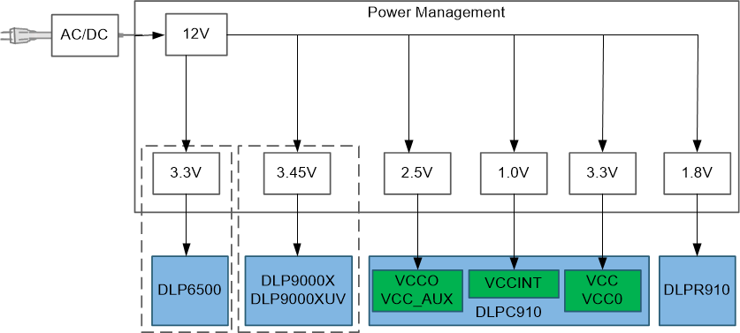
The DLPC910, the DLPR910, and one of the DLP9000X, DLP9000XUV, or DLP6500 DMDs are powered by a power distribution method as shown in Figure 9-1. The DMD power inputs will depend on which DMD is being used in the application.
GUID-75699BE5-D5B1-4742-98D4-C9B74CD880C5-low.gifFigure 9-1 Power Distribution