ZHCSE90D September 2015 – September 2020 DLPC910
PRODUCTION DATA
- 1 特性
- 2 应用
- 3 说明
- 4 Revision History
- 5 Pin Configuration and Functions
- 6 Specifications
-
7 Detailed Description
- 7.1 Overview
- 7.2 Functional Block Diagram
- 7.3 Feature Description
- 7.4 Device Functional Modes
- 7.5
Register Map
- 7.5.1
Register Table Overview
- 7.5.1.1 DESTOP_INTERRUPT Register
- 7.5.1.2 MAIN_STATUS Register
- 7.5.1.3 DESTOP_CAL Register
- 7.5.1.4 DESTOP_DMD_ID_REG Register
- 7.5.1.5 DESTOP_CATBITS_REG Register
- 7.5.1.6 DESTOP_VERSION Register
- 7.5.1.7 DESTOP_RESET_REG Register
- 7.5.1.8 DESTOP_INFIFO_STATUS Register
- 7.5.1.9 DESTOP_BUS_SWAP Register
- 7.5.1.10 DESTOP_DMDCTRL Register
- 7.5.1.11 DESTOP_BIT_FLIP Register
- 7.5.1
Register Table Overview
- 8 Application and Implementation
- 9 Power Supply Recommendations
- 10Layout
- 11Device and Documentation Support
- 12Mechanical, Packaging, and Orderable Information
7.4.1.1 Data and Command Write Cycle
Once initialization completes (INIT_ACTIVE = 0), the user is free to send bit plane data and control information to the DLPC910. The row write cycle begins with the assertion of DVALID. DVALID, all bit plane data, and all DMD control information must be presented to the DLPC910 synchronous to the input clock DCLKIN. When the user asserts a DVALID signal, the DLPC910 begins sampling the LVDS data inputs and control inputs and synchronously sends this information to the DMD along with row address control information.
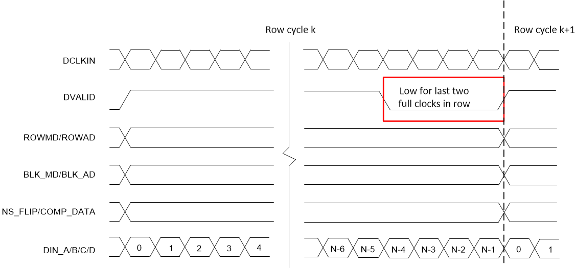
The DMD incorporates single row write operations using a row address counter that is randomly addressable. The Row Mode and Row address must be presented synchronous to the DCLKIN at this beginning of each row cycle. As shown in Table 7-1 and Table 7-2, ROWMD(1:0) determines the single row write count mode and ROWAD(10:0) determines the single row write address. ROWMD and ROWAD must be asserted synchronously with DVALID and must be valid synchronous to the beginning of the bit plane data as shown in Figure 7-6.
Figure 7-6 shows an example of data written to the DLPC910 for two consecutive row cycles. This diagram applies to the DLPC910 for all compatible DMDs with a difference between DMD bus widths and number of clock cycles per row. For the DLP9000X/DLP9000XUV DMDs, data is written to the DLPC910 64 bits on each clock edge (16 Bus A bits + 16 Bus B bits + 16 Bus C bits + 16 Bus D bits) for 20 clock cycles (N=40) to complete one row cycle. For the DLP6500 DMD, only Bus A and Bus B are used (32 bits total) for 32 clock cycles (N=64) to complete one row cycle. An entire row of data must be written for data to be properly latched into the DMD memory. To complete the first row cycle (k), DVALID should be de-asserted (logic '0') two full clock cycles prior to the completion of the row cycle. The assertion of DVALID back high ('1') indicates the beginning of the next row cycle (k+1). For non-consecutive row cycles, keep DVALID low until the next row cycles is to begin, at which point DVALID should be taken high to start the next row cycle. This is for all row cycle operations including No-Op row cycles.
Setting DVALID to LOW for the last clock cycle does not affect data read in the last two clock transitions. The firmware will finish the correct number data reads from DIN_(A/B/C/D) for the specific DMD, started by the rising edge of DVALID at the beginning of the row cycle.
 Figure 7-6 DLPC910 Input Consecutive Single Row Write Cycles