ZHCSFD6G july 2016 – august 2023 DP83822H , DP83822HF , DP83822I , DP83822IF
PRODUCTION DATA
- 1
- 1 特性
- 2 应用
- 3 说明
- 4 Revision History
- 5 Device Comparison Table
- 6 Pin Configuration and Functions
-
7 Specifications
- 7.1 Absolute Maximum Ratings
- 7.2 ESD Ratings
- 7.3 Recommended Operating Conditions
- 7.4 Thermal Information
- 7.5 Electrical Characteristics
- 7.6 Timing Requirements, Power-Up Timing
- 7.7 Timing Requirements, Power-Up With Unstable XI Clock
- 7.8 Timing Requirements, Reset Timing
- 7.9 Timing Requirements, Serial Management Timing
- 7.10 Timing Requirements, 100 Mbps MII Transmit Timing
- 7.11 Timing Requirements, 100 Mbps MII Receive Timing
- 7.12 Timing Requirements, 10 Mbps MII Transmit Timing
- 7.13 Timing Requirements, 10 Mbps MII Receive Timing
- 7.14 Timing Requirements, RMII Transmit Timing
- 7.15 Timing Requirements, RMII Receive Timing
- 7.16 Timing Requirements, RGMII
- 7.17 Normal Link Pulse Timing
- 7.18 Auto-Negotiation Fast Link Pulse (FLP) Timing
- 7.19 10BASE-Te Jabber Timing
- 7.20 100BASE-TX Transmit Latency Timing
- 7.21 100BASE-TX Receive Latency Timing
- 7.22 Timing Diagrams
- 7.23 Typical Characteristics
-
8 Detailed Description
- 8.1 Overview
- 8.2 Functional Block Diagram
- 8.3 Feature Description
- 8.4
Device Functional Modes
- 8.4.1 MAC Interfaces
- 8.4.2
Serial Management Interface
- 8.4.2.1 Extended Register Space Access
- 8.4.2.2 Write Address Operation
- 8.4.2.3 Read Address Operation
- 8.4.2.4 Write (No Post Increment) Operation
- 8.4.2.5 Read (No Post Increment) Operation
- 8.4.2.6 Write (Post Increment) Operation
- 8.4.2.7 Read (Post Increment) Operation
- 8.4.2.8 Example Write Operation (No Post Increment)
- 8.4.2.9 Example Read Operation (No Post Increment)
- 8.4.3 100BASE-TX
- 8.4.4 100BASE-FX
- 8.4.5 10BASE-Te
- 8.4.6 Auto-Negotiation (Speed / Duplex Selection)
- 8.4.7 Auto-MDIX Resolution
- 8.4.8 Loopback Modes
- 8.4.9 BIST Configurations
- 8.4.10 Cable Diagnostics
- 8.4.11 Fast Link Down Functionality
- 8.5 Programming
- 8.6 Register Maps
- 9 Application and Implementation
- 10Power Supply Recommendations
- 11Layout
- 12Device and Documentation Support
- 13Mechanical, Packaging, and Orderable Information
8.4.11 Fast Link Down Functionality
The DP83822 includes advanced link-down capabilities that support various real-time applications. The link-down mechanism is configurable and includes enhanced modes that allow extremely fast link-drop reaction times.
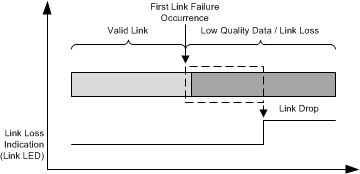
The DP83822 supports an enhanced link drop mechanism, also called Fast Link Drop (FLD), which shortens the observation window for determining link. There are multiple ways of determining link status, which can be enabled or disabled based on user preference. Fast Link Drop can be enabled in hardware with bootstrapping or in software using register configuration. RX_D2 when strapped to either mode 2 or mode 3 will enable FLD at power up or hardware reset. Additionally, FLD can be configured using the Control Register #3 (CR3, address 0x000B). Bits[3:0] and bit[10] allow for various FLD conditions to be enabled. When link drop occurs, indication of a particular fault condition can be read from the Fast Link Down Status Register (FLDS, address 0x000F).
 Figure 8-9 Fast Link Down
Fast Link Down criteria include:
- RX Error Count - when a predefined number of 32 RX_ERs occur in a 10μs window, the link will be dropped.
- MLT3 Error Count - when a predefined number of 20 MLT3 errors occur in a 10μs window, the link will be dropped.
- Low SNR Threshold - when a predefined number of 20 threshold crossings occur in a 10μs window, the link will be dropped.
- Signal/Energy Loss - when the energy detector indicates energy loss, the link will be dropped.
The Fast Link Down functionality allows the use of each of these options separately or in any combination.
Because this mode enables extremely quick reaction time, it is more exposed to temporary bad link-quality scenarios.