ZHCSFD6G july 2016 – august 2023 DP83822H , DP83822HF , DP83822I , DP83822IF
PRODUCTION DATA
- 1
- 1 特性
- 2 应用
- 3 说明
- 4 Revision History
- 5 Device Comparison Table
- 6 Pin Configuration and Functions
-
7 Specifications
- 7.1 Absolute Maximum Ratings
- 7.2 ESD Ratings
- 7.3 Recommended Operating Conditions
- 7.4 Thermal Information
- 7.5 Electrical Characteristics
- 7.6 Timing Requirements, Power-Up Timing
- 7.7 Timing Requirements, Power-Up With Unstable XI Clock
- 7.8 Timing Requirements, Reset Timing
- 7.9 Timing Requirements, Serial Management Timing
- 7.10 Timing Requirements, 100 Mbps MII Transmit Timing
- 7.11 Timing Requirements, 100 Mbps MII Receive Timing
- 7.12 Timing Requirements, 10 Mbps MII Transmit Timing
- 7.13 Timing Requirements, 10 Mbps MII Receive Timing
- 7.14 Timing Requirements, RMII Transmit Timing
- 7.15 Timing Requirements, RMII Receive Timing
- 7.16 Timing Requirements, RGMII
- 7.17 Normal Link Pulse Timing
- 7.18 Auto-Negotiation Fast Link Pulse (FLP) Timing
- 7.19 10BASE-Te Jabber Timing
- 7.20 100BASE-TX Transmit Latency Timing
- 7.21 100BASE-TX Receive Latency Timing
- 7.22 Timing Diagrams
- 7.23 Typical Characteristics
-
8 Detailed Description
- 8.1 Overview
- 8.2 Functional Block Diagram
- 8.3 Feature Description
- 8.4
Device Functional Modes
- 8.4.1 MAC Interfaces
- 8.4.2
Serial Management Interface
- 8.4.2.1 Extended Register Space Access
- 8.4.2.2 Write Address Operation
- 8.4.2.3 Read Address Operation
- 8.4.2.4 Write (No Post Increment) Operation
- 8.4.2.5 Read (No Post Increment) Operation
- 8.4.2.6 Write (Post Increment) Operation
- 8.4.2.7 Read (Post Increment) Operation
- 8.4.2.8 Example Write Operation (No Post Increment)
- 8.4.2.9 Example Read Operation (No Post Increment)
- 8.4.3 100BASE-TX
- 8.4.4 100BASE-FX
- 8.4.5 10BASE-Te
- 8.4.6 Auto-Negotiation (Speed / Duplex Selection)
- 8.4.7 Auto-MDIX Resolution
- 8.4.8 Loopback Modes
- 8.4.9 BIST Configurations
- 8.4.10 Cable Diagnostics
- 8.4.11 Fast Link Down Functionality
- 8.5 Programming
- 8.6 Register Maps
- 9 Application and Implementation
- 10Power Supply Recommendations
- 11Layout
- 12Device and Documentation Support
- 13Mechanical, Packaging, and Orderable Information
8.4.1.2 Reduced Media Independent Interface (RMII)
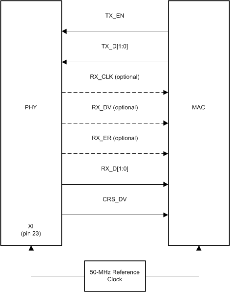
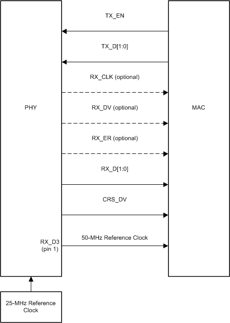
The DP83822 incorporates the Reduced Media Independent Interface (RMII) as specified in the RMII specification from the RMII consortium. The purpose of this interface is to provide a reduced pin count alternative to the IEEE 802.3u MII as specified in Clause 22. Architecturally, the RMII specification provides an additional reconciliation layer on either side of the MII, but can be implemented in the absence of an MII. The DP83822 offers two types of RMII operations: RMII Slave and RMII Master. In RMII Slave operation, the DP83822 operates off of a 50-MHz CMOS-level oscillator connected to the XI pin and shares the same clock as the MAC. In RMII Master operation, the DP83822 operates off of either a 25-MHz CMOS-level oscillator connected to XI pin or a 25-MHz crystal connected across XI and XO pins. A 50-MHz output clock referenced from any of the three DP83822 GPIOs is connected to the MAC.
If RMII Master mode is configured through bootstraps, a 50-MHz output clock will automatically be enabled on RX_D3 (GPIO3).
The RMII specification has the following characteristics:
- Supports 100BASE-FX, 100BASE-TX and 10BASE-Te.
- Single clock reference sourced from the MAC to PHY (or from an external source)
- Provides independent 2-bit wide transmit and receive data paths
- Uses CMOS signal levels, the same levels as the MII interface
In this mode, data transfers are two bits for every clock cycle using the internal 50-MHz reference clock for both transmit and receive paths.
The RMII signals are summarized below:
| FUNCTION | PINS |
|---|---|
| Data Signals | TX_D[1:0] |
| RX_D[1:0] | |
| Transmit and Receive Signals | TX_EN |
| CRS_DV |
 Figure 8-5 RMII Slave Signaling
 Figure 8-6 RMII Master Signaling
Data on TX_D[1:0] are latched at the PHY with reference to the clock edges on the XI pin. Data on RX_D[1:0] are latched at the MAC with reference to the same clock edges on the XI pin. RMII operates at the same speed in 10BASE-Te, 100BASE-TX and 100BASE-FX. In 10BASE-Te the data is 10 times slower than the reference clock, so transmit data is sampled every 10 clock cycles. Likewise, receive data is generated on every 10th clock so that an attached MAC device can sample the data every 10 clock cycles.
In addition, RMII mode supplies an RX_DV signal that allows a simpler method of recovering receive data without the need to separate RX_DV from the CRS_DV indication. RX_ER is also supported even though it is not required by the RMII specification.
RMII includes a programmable elastic buffer to adjust for the frequency differences between the reference clock and the recovered receive clock. The programmable elastic buffer minimizes internal propagation delay based on expected maximum packet size and clock accuracy.
Table below indicates how to program the buffer FIFO based on the expected maximum packet size and clock accuracy. It assumes that the RMII reference clock and the far-end transmitter clock have the same accuracy.
| START THRESHOLD RBR[1:0] | LATENCY TOLERANCE | RECOMMENDED PACKET SIZE AT ±50 ppm | RECOMMENDED PACKET SIZE AT ±100 ppm |
|---|---|---|---|
| 1 (4-bits) | 2 bits | 2400 bytes | 1200 bytes |
| 2 (8-bits) | 6 bits | 7200 bytes | 3600 bytes |
| 3 (12-bits) | 10 bits | 12000 bytes | 6000 bytes |
| 4 (16-bits) | 14 bits | 16800 bytes | 8400 bytes |