ZHCSJ67A December 2018 – August 2019 DP83825I
PRODUCTION DATA.
- 1 特性
- 2 应用
- 3 说明
- 4 修订历史记录
- 5 Pin Configuration and Functions
- 6 Specifications
-
7 Detailed Description
- 7.1 Overview
- 7.2 Functional Block Diagram
- 7.3
Feature Description
- 7.3.1 Auto-Negotiation (Speed / Duplex Selection)
- 7.3.2 Auto-MDIX Resolution
- 7.3.3 Energy Efficient Ethernet
- 7.3.4 EEE for Legacy MACs Not Supporting 802.3az
- 7.3.5 Wake-on-LAN Packet Detection
- 7.3.6 Low Power Modes
- 7.3.7 IEEE Power Down
- 7.3.8 Deep Power Down
- 7.3.9 RMII Repeater Mode
- 7.3.10 Reduced Media Independent Interface (RMII)
- 7.3.11
Serial Management Interface
- 7.3.11.1 Extended Register Space Access
- 7.3.11.2 Write Address Operation
- 7.3.11.3 Read Address Operation
- 7.3.11.4 Write (No Post Increment) Operation
- 7.3.11.5 Read (No Post Increment) Operation
- 7.3.11.6 Write (Post Increment) Operation
- 7.3.11.7 Read (Post Increment) Operation
- 7.3.11.8 Example Write Operation (No Post Increment)
- 7.3.11.9 Example Read Operation (No Post Increment)
- 7.3.12 100BASE-TX
- 7.3.13 10BASE-Te
- 7.3.14 Loopback Modes
- 7.3.15 BIST Configurations
- 7.3.16 Cable Diagnostics
- 7.3.17 Single Voltage Supply
- 7.4 Device Functional Modes
- 7.5 Programming
- 7.6
Register Maps
- 7.6.1 BMCR_Register Register (Offset = 0x0) [reset = 0x3100]
- 7.6.2 BMSR_Register Register (Offset = 0x1) [reset = 0x7849]
- 7.6.3 PHYIDR1_Register Register (Offset = 0x2) [reset = 0x2000]
- 7.6.4 PHYIDR2_Register Register (Offset = 0x3) [reset = 0xA140]
- 7.6.5 ANAR_Register Register (Offset = 0x4) [reset = 0x1E1]
- 7.6.6 ALNPAR_Register Register (Offset = 0x5) [reset = 0x0]
- 7.6.7 ANER_Register Register (Offset = 0x6) [reset = 0x4]
- 7.6.8 ANNPTR_Register Register (Offset = 0x7) [reset = 0x2001]
- 7.6.9 ANLNPTR_Register Register (Offset = 0x8) [reset = 0x0]
- 7.6.10 CR1_Register Register (Offset = 0x9) [reset = 0x0]
- 7.6.11 CR2_Register Register (Offset = 0xA) [reset = 0x0]
- 7.6.12 CR3_Register Register (Offset = 0xB) [reset = 0x0]
- 7.6.13 Register_12 Register (Offset = 0xC) [reset = 0x0]
- 7.6.14 REGCR_Register Register (Offset = 0xD) [reset = 0x0]
- 7.6.15 ADDAR_Register Register (Offset = 0xE) [reset = 0x0]
- 7.6.16 FLDS_Register Register (Offset = 0xF) [reset = 0x0]
- 7.6.17 PHYSTS_Register Register (Offset = 0x10) [reset = 0x0]
- 7.6.18 PHYSCR_Register Register (Offset = 0x11) [reset = 0x108]
- 7.6.19 MISR1_Register Register (Offset = 0x12) [reset = 0x0]
- 7.6.20 MISR2_Register Register (Offset = 0x13) [reset = 0x0]
- 7.6.21 FCSCR_Register Register (Offset = 0x14) [reset = 0x0]
- 7.6.22 RECR_Register Register (Offset = 0x15) [reset = 0x0]
- 7.6.23 BISCR_Register Register (Offset = 0x16) [reset = 0x100]
- 7.6.24 RCSR_Register Register (Offset = 0x17) [reset = 0x1]
- 7.6.25 LEDCR_Register Register (Offset = 0x18) [reset = 0x400]
- 7.6.26 PHYCR_Register Register (Offset = 0x19) [reset = 0x8000]
- 7.6.27 10BTSCR_Register Register (Offset = 0x1A) [reset = 0x0]
- 7.6.28 BICSR1_Register Register (Offset = 0x1B) [reset = 0x7D]
- 7.6.29 BICSR2_Register Register (Offset = 0x1C) [reset = 0x5EE]
- 7.6.30 CDCR_Register Register (Offset = 0x1E) [reset = 0x0]
- 7.6.31 PHYRCR_Register Register (Offset = 0x1F) [reset = 0x0]
- 7.6.32 MLEDCR_Register Register (Offset = 0x25) [reset = 0x41]
- 7.6.33 COMPT_Regsiter Register (Offset = 0x27) [reset = 0x0]
- 7.6.34 Register_101 Register (Offset = 0x101) [reset = 0x2082]
- 7.6.35 Register_10a Register (Offset = 0x10A) [reset = 0x2040]
- 7.6.36 Register_123 Register (Offset = 0x123) [reset = 0x51C]
- 7.6.37 Register_130 Register (Offset = 0x130) [reset = 0x4F28]
- 7.6.38 CDSCR_Register Register (Offset = 0x170) [reset = 0x410]
- 7.6.39 CDSCR2_Register Register (Offset = 0x171) [reset = 0x0]
- 7.6.40 TDR_172_Register Register (Offset = 0x172) [reset = 0x0]
- 7.6.41 CDSCR3_Register Register (Offset = 0x173) [reset = 0x1304]
- 7.6.42 TDR_174_Register Register (Offset = 0x174) [reset = 0x0]
- 7.6.43 TDR_175_Register Register (Offset = 0x175) [reset = 0x1004]
- 7.6.44 TDR_176_Register Register (Offset = 0x176) [reset = 0x5]
- 7.6.45 CDSCR4_Register Register (Offset = 0x177) [reset = 0x1E00]
- 7.6.46 TDR_178_Register Register (Offset = 0x178) [reset = 0x2]
- 7.6.47 CDLRR1_Register Register (Offset = 0x180) [reset = 0x0]
- 7.6.48 CDLRR2_Register Register (Offset = 0x181) [reset = 0x0]
- 7.6.49 CDLRR3_Register Register (Offset = 0x182) [reset = 0x0]
- 7.6.50 CDLRR4_Register Register (Offset = 0x183) [reset = 0x0]
- 7.6.51 CDLRR5_Register Register (Offset = 0x184) [reset = 0x0]
- 7.6.52 CDLAR1_Register Register (Offset = 0x185) [reset = 0x0]
- 7.6.53 CDLAR2_Register Register (Offset = 0x186) [reset = 0x0]
- 7.6.54 CDLAR3_Register Register (Offset = 0x187) [reset = 0x0]
- 7.6.55 CDLAR4_Register Register (Offset = 0x188) [reset = 0x0]
- 7.6.56 CDLAR5_Register Register (Offset = 0x189) [reset = 0x0]
- 7.6.57 CDLAR6_Register Register (Offset = 0x18A) [reset = 0x0]
- 7.6.58 IO_CFG_Register Register (Offset = 0x302) [reset = 0x0]
- 7.6.59 SPARE_OUT Register (Offset = 0x308) [reset = 0x2]
- 7.6.60 DAC_CFG_0 Register (Offset = 0x30B) [reset = 0xC00]
- 7.6.61 DAC_CFG_1 Register (Offset = 0x30C) [reset = 0x20]
- 7.6.62 DSP_CFG_0 Register (Offset = 0x30F) [reset = 0x464]
- 7.6.63 DSP_CFG_2 Register (Offset = 0x311) [reset = 0x1FC]
- 7.6.64 DSP_CFG_4 Register (Offset = 0x313) [reset = 0x6F8]
- 7.6.65 DSP_CFG_13 Register (Offset = 0x31C) [reset = 0x1101]
- 7.6.66 DSP_CFG_16 Register (Offset = 0x31F) [reset = 0xFC36]
- 7.6.67 DSP_CFG_25 Register (Offset = 0x33C) [reset = 0xEC00]
- 7.6.68 DSP_CFG_27 Register (Offset = 0x33E) [reset = 0x261E]
- 7.6.69 ANA_LD_PROG_SL_Register Register (Offset = 0x404) [reset = 0x80]
- 7.6.70 ANA_RX10BT_CTRL_Register Register (Offset = 0x40D) [reset = 0x0]
- 7.6.71 Register_416 Register (Offset = 0x416) [reset = 0x830]
- 7.6.72 Register_429 Register (Offset = 0x429) [reset = 0x0]
- 7.6.73 GENCFG_Register Register (Offset = 0x456) [reset = 0x8]
- 7.6.74 LEDCFG_Register Register (Offset = 0x460) [reset = 0x10]
- 7.6.75 IOCTRL_Register Register (Offset = 0x461) [reset = 0x0]
- 7.6.76 SOR1_Register Register (Offset = 0x467) [reset = 0x101]
- 7.6.77 SOR2_Register Register (Offset = 0x468) [reset = 0x80]
- 7.6.78 Register_0x469_Register Register (Offset = 0x469) [reset = 0x40]
- 7.6.79 RXFCFG_Register Register (Offset = 0x4A0) [reset = 0x1081]
- 7.6.80 RXFS_Register Register (Offset = 0x4A1) [reset = 0x1000]
- 7.6.81 RXFPMD1_Register Register (Offset = 0x4A2) [reset = 0x0]
- 7.6.82 RXFPMD2_Register Register (Offset = 0x4A3) [reset = 0x0]
- 7.6.83 RXFPMD3_Register Register (Offset = 0x4A4) [reset = 0x0]
- 7.6.84 Register_0x4cd Register (Offset = 0x4CD) [reset = 0x408]
- 7.6.85 Register_0x4ce Register (Offset = 0x4CE) [reset = 0x12]
- 7.6.86 Register_0x4cf Register (Offset = 0x4CF) [reset = 0x261D]
- 7.6.87 EEECFG2_Register Register (Offset = 0x4D0) [reset = 0x0]
- 7.6.88 EEECFG3_Register Register (Offset = 0x4D1) [reset = 0x18B]
- 7.6.89 Register_0x4d2 Register (Offset = 0x4D2) [reset = 0x354A]
- 7.6.90 Register_0x4d4 Register (Offset = 0x4D4) [reset = 0x6633]
- 7.6.91 DSP_100M_STEP_2_Register Register (Offset = 0x4D5) [reset = 0x2F1]
- 7.6.92 DSP_100M_STEP_3_Register Register (Offset = 0x4D6) [reset = 0x171]
- 7.6.93 DSP_100M_STEP_4_Register Register (Offset = 0x4D7) [reset = 0x171]
- 7.6.94 MMD3_PCS_CTRL_1_Register Register (Offset = 0x1000) [reset = 0x0]
- 7.6.95 MMD3_PCS_STATUS_1 Register (Offset = 0x1001) [reset = 0x40]
- 7.6.96 MMD3_EEE_CAPABILITY_Register Register (Offset = 0x1014) [reset = 0x2]
- 7.6.97 MMD3_WAKE_ERR_CNT_Register Register (Offset = 0x1016) [reset = 0x0]
- 7.6.98 MMD7_EEE_ADVERTISEMENT_Register Register (Offset = 0x203C) [reset = 0x0]
- 7.6.99 MMD7_EEE_LP_ABILITY_Register Register (Offset = 0x203D) [reset = 0x0]
- 8 Application and Implementation
- 9 Power Supply Recommendations
- 10Layout
- 11器件和文档支持
- 12机械、封装和可订购信息
7.3.10 Reduced Media Independent Interface (RMII)
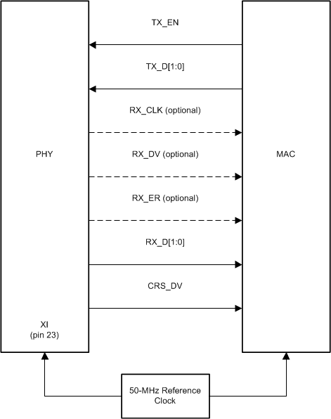
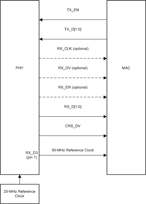
The DP83825I incorporates the Reduced Media Independent Interface (RMII) as specified in the RMII specification v1.2. The purpose of this interface is to provide a reduced pin count alternative to the IEEE 802.3 MII as specified in Clause 22. Architecturally, the RMII specification provides an additional reconciliation layer on either side of the MII, but can be implemented in the absence of an MII. The DP83825I offers two types of RMII operations: RMII Slave and RMII Master. In RMII Master operation, the DP83825I operates off either a 25-MHz CMOS-level oscillator connected to XI pin or a 25-MHz crystal connected across XI and XO pins. A 50-MHz output clock referenced from DP83825I can be connected to the MAC. In RMII Slave operation, the DP83825I operates off of a 50-MHz CMOS-level oscillator connected to the XI pin and shares the same clock as the MAC. Alternatively, in RMII Slave mode, the PHY can run from 50MHz clock provided by the Host MAC.
The RMII specification has the following characteristics:
- Supports 100BASE-TX and 10BASE-Te.
- Single clock reference sourced from the MAC to PHY (or from an external source)
- Provides independent 2-bit wide transmit and receive data paths
- Uses CMOS signal levels, the same levels as the MII interface
In this mode, data transfers are two bits for every clock cycle using the internal 50-MHz reference clock for both transmit and receive paths.
The RMII signals are summarized in Table 1:
Table 1. RMII Signals
| FUNCTION | PINS |
|---|---|
| Receive Data Lines | TX_D[1:0] |
| Transmit Data Lines | RX_D[1:0] |
| Receive Control Signal | TX_EN |
| Transmit Control Signal | CRS_DV |
 Figure 12. RMII Slave Signaling
  Figure 13. RMII Master Signaling
 Data on TX_D[1:0] are latched at the PHY with reference to the clock edges on the XI pin. Data on RX_D[1:0] are latched at the MAC with reference to the same clock edges on the XI pin.
In addition, CRX_DV can be configured as RX_DV signal. It allows a simpler method of recovering received data without the need to separate RX_DV from the CRS_DV indication.