ZHCSKM7G december 2019 – july 2023 DP83826E , DP83826I
PRODUCTION DATA
- 1
- 1 特性
- 2 应用
- 3 说明
- 4 Revision History
- 5 Mode Comparison Tables
- 6 Pin Configuration and Functions (ENHANCED Mode)
- 7 Pin Configuration and Functions (BASIC Mode)
- 8 Specifications
-
9 Detailed Description
- 9.1 Overview
- 9.2 Functional Block Diagram
- 9.3
Feature Description
- 9.3.1 Auto-Negotiation (Speed/Duplex Selection)
- 9.3.2 Auto-MDIX Resolution
- 9.3.3 Energy Efficient Ethernet
- 9.3.4 EEE for Legacy MACs Not Supporting 802.3az
- 9.3.5 Wake-on-LAN Packet Detection
- 9.3.6 Low Power Modes
- 9.3.7 RMII Repeater Mode
- 9.3.8 Clock Output
- 9.3.9 Media Independent Interface (MII)
- 9.3.10 Reduced Media Independent Interface (RMII)
- 9.3.11 Serial Management Interface
- 9.3.12 100BASE-TX
- 9.3.13 10BASE-Te
- 9.3.14 Loopback Modes
- 9.3.15 BIST Configurations
- 9.3.16 Cable Diagnostics
- 9.3.17 LED and GPIO Configuration
- 9.4 Programming
- 9.5 Register Maps
- 10Application and Implementation
- 11Power Supply Recommendations
- 12Layout
- 13Device and Documentation Support
- 14Mechanical, Packaging, and Orderable Information
9.3.10 Reduced Media Independent Interface (RMII)
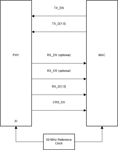
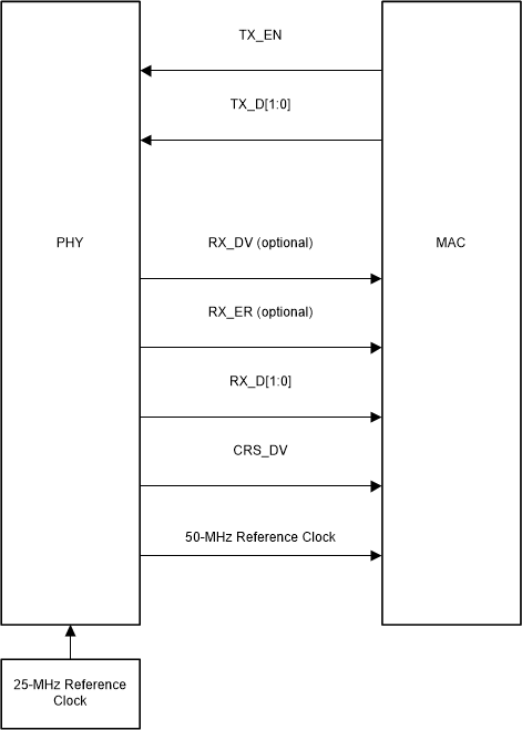
The DP83826 incorporates the reduced media-independent interface (RMII) as specified in the RMII specification v1.2. The purpose of this interface is to provide a reduced pin count alternative to the IEEE 802.3 MII as specified in Clause 22. Architecturally, the RMII specification provides an additional reconciliation layer on either side of the MII, but can be implemented in the absence of an MII. The DP83826 offers two types of RMII operations: RMII Slave and RMII Master. In RMII Master operation, the DP83826 operates from either a 25-MHz CMOS-level oscillator connected to XI pin, a 25-MHz crystal connected across XI and XO pins. A 50-MHz output clock referenced from DP83826 can be connected to the MAC. In RMII Slave operation, the DP83826 operates from a 50-MHz CMOS-level oscillator connected to the XI pin and shares the same clock as the MAC. Alternatively, in RMII slave mode, the PHY can operate from a 50-MHz clock provided by the Host MAC
The RMII specification has the following characteristics:
- Supports 100BASE-TX and 10BASE-Te
- Single clock reference sourced from the MAC to PHY (or from an external source)
- Provides independent 2-bit wide transmit and receive data paths
- Uses CMOS signal levels, the same levels as the MII interface
In this mode, data transfers are 2 bits for every clock cycle using the internal 50-MHz reference clock for both transmit and receive paths.
The RMII signals are summarized below:
| FUNCTION | PINS |
|---|---|
| Receive data lines | TX_D[1:0] |
| Transmit data lines | RX_D[1:0] |
| Receive control signal | TX_EN |
| Transmit control signal | CRS_DV |
 Figure 9-5 RMII Slave Signaling
 Figure 9-6 RMII Master Signaling
Data on TX_D[1:0] are latched at the PHY with reference to the 50 MHz-clock in RMII master mode and slave mode. Data on RX_D[1:0] is provided in reference to 50-MHz clock.
In addition, CRX_DV can be configured as RX_DV signal. It allows a simpler method of recovering receive data without the need to separate RX_DV from the CRS_DV indication.