ZHCSKM7G december   2019  – july 2023 DP83826E , DP83826I

PRODUCTION DATA  

  1.   1
  2. 特性
  3. 应用
  4. 说明
  5. Revision History
  6. Mode Comparison Tables
  7. Pin Configuration and Functions (ENHANCED Mode)
  8. Pin Configuration and Functions (BASIC Mode)
  9. Specifications
    1. 8.1 绝对最大额定值
    2. 8.2 ESD 等级
    3. 8.3 建议运行条件
    4. 8.4 热性能信息
    5. 8.5 电气特性
    6. 8.6 时序要求
    7. 8.7 Timing Diagrams
    8. 8.8 Typical Characteristics
  10. Detailed Description
    1. 9.1 Overview
    2. 9.2 Functional Block Diagram
    3. 9.3 Feature Description
      1. 9.3.1  Auto-Negotiation (Speed/Duplex Selection)
      2. 9.3.2  Auto-MDIX Resolution
      3. 9.3.3  Energy Efficient Ethernet
        1. 9.3.3.1 EEE Overview
        2. 9.3.3.2 EEE Negotiation
      4. 9.3.4  EEE for Legacy MACs Not Supporting 802.3az
      5. 9.3.5  Wake-on-LAN Packet Detection
        1. 9.3.5.1 Magic Packet Structure
        2. 9.3.5.2 Magic Packet Example
        3. 9.3.5.3 Wake-on-LAN Configuration and Status
      6. 9.3.6  Low Power Modes
        1. 9.3.6.1 Active Sleep
        2. 9.3.6.2 IEEE Power-Down
        3. 9.3.6.3 Deep Power Down State
      7. 9.3.7  RMII Repeater Mode
      8. 9.3.8  Clock Output
      9. 9.3.9  Media Independent Interface (MII)
      10. 9.3.10 Reduced Media Independent Interface (RMII)
      11. 9.3.11 Serial Management Interface
        1. 9.3.11.1 Extended Register Space Access
        2. 9.3.11.2 Write Address Operation
        3. 9.3.11.3 Read Address Operation
        4. 9.3.11.4 Write (No Post Increment) Operation
        5. 9.3.11.5 Read (No Post Increment) Operation
        6. 9.3.11.6 Example Write Operation (No Post Increment)
      12. 9.3.12 100BASE-TX
        1. 9.3.12.1 100BASE-TX Transmitter
          1. 9.3.12.1.1 Code-Group Encoding and Injection
          2. 9.3.12.1.2 Scrambler
          3. 9.3.12.1.3 NRZ to NRZI Encoder
          4. 9.3.12.1.4 Binary to MLT-3 Converter
        2. 9.3.12.2 100BASE-TX Receiver
      13. 9.3.13 10BASE-Te
        1. 9.3.13.1 Squelch
        2. 9.3.13.2 Normal Link Pulse Detection and Generation
        3. 9.3.13.3 Jabber
        4. 9.3.13.4 Active Link Polarity Detection and Correction
      14. 9.3.14 Loopback Modes
        1. 9.3.14.1 Near-end Loopback
        2. 9.3.14.2 MII Loopback
        3. 9.3.14.3 PCS Loopback
        4. 9.3.14.4 Digital Loopback
        5. 9.3.14.5 Analog Loopback
        6. 9.3.14.6 Far-End (Reverse) Loopback
      15. 9.3.15 BIST Configurations
      16. 9.3.16 Cable Diagnostics
        1. 9.3.16.1 Time Domain Reflectometry (TDR)
        2. 9.3.16.2 Fast Link-Drop Functionality
      17. 9.3.17 LED and GPIO Configuration
    4. 9.4 Programming
      1. 9.4.1 Hardware Bootstraps Configuration
        1. 9.4.1.1 DP83826 Bootstrap Configurations (ENHANCED Mode)
          1. 9.4.1.1.1 Bootstraps for PHY Address
        2. 9.4.1.2 DP83826 Strap Configuration (BASIC Mode)
          1. 9.4.1.2.1 Bootstraps for PHY Address
    5. 9.5 Register Maps
      1. 9.5.1 DP83826 Registers
  11. 10Application and Implementation
    1. 10.1 Application Information
    2. 10.2 Typical Applications
      1. 10.2.1 Twisted-Pair Interface (TPI) Network Circuit
      2. 10.2.2 Transformer Recommendations
      3. 10.2.3 Capacitive DC Blocking
      4. 10.2.4 Design Requirements
        1. 10.2.4.1 Clock Requirements
          1. 10.2.4.1.1 Oscillator
          2. 10.2.4.1.2 Crystal
      5. 10.2.5 Detailed Design Procedure
        1. 10.2.5.1 MII Layout Guidelines
        2. 10.2.5.2 RMII Layout Guidelines
        3. 10.2.5.3 MDI Layout Guidelines
      6. 10.2.6 Application Curves
  12. 11Power Supply Recommendations
  13. 12Layout
    1. 12.1 Layout Guidelines
      1. 12.1.1 Signal Traces
      2. 12.1.2 Return Path
      3. 12.1.3 Transformer Layout
      4. 12.1.4 Metal Pour
      5. 12.1.5 PCB Layer Stacking
        1. 12.1.5.1 Layout Example
  14. 13Device and Documentation Support
    1. 13.1 Related Documentation
    2. 13.2 Receiving Notification of Documentation Updates
    3. 13.3 Support Resources
    4. 13.4 Trademarks
    5. 13.5 静电放电警告
    6. 13.6 术语表
  15. 14Mechanical, Packaging, and Orderable Information

封装选项

机械数据 (封装 | 引脚)
散热焊盘机械数据 (封装 | 引脚)
订购信息

Hardware Bootstraps Configuration

DP83826 uses many of the functional pins as strap options to place the device into specific modes of operation. The values of these pins are sampled at power up or hard reset. During software resets, the strap options are internally reloaded from the values sampled at power up or hard reset. The strap option pin assignments are defined below. Configuration of the device may be done through the strap pins or through the management register interface. A pullup resistor or a pulldown resistor of suggested values may be used to set the voltage ratio of the strap pin input and the supply to select one of the possible selected modes. All strap pins have two levels.
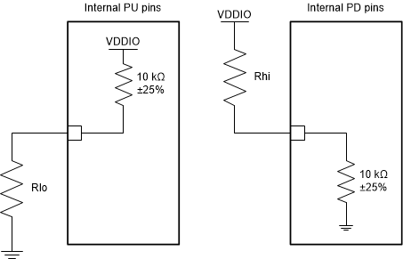
GUID-0B20D17D-2E89-42E8-B6A4-0C777A2221CE-low.gifFigure 9-10 Strap Circuit
Table 9-6 2-Level Strap Resistor Ratios
Mode (1)SUGGESTED RESISTORS
RHI (kΩ)RLO (kΩ)
INTERNAL 10-kΩ PULLDOWN (PD) PINS
0-DEFAULTOPENOPEN
12.49OPEN
INTERNAL 10-kΩ PULLUP (PU) PINS
0OPEN1.5
1-DEFAULTOPENOPEN
Resistor ratios are only a recommendation. Use the bootstrap threshold values contained within the Electrical Characteristics table for more precise mode selections. Recommended tolerance is 1%.