ZHCSKM7G december   2019  – july 2023 DP83826E , DP83826I

PRODUCTION DATA  

  1.   1
  2. 特性
  3. 应用
  4. 说明
  5. Revision History
  6. Mode Comparison Tables
  7. Pin Configuration and Functions (ENHANCED Mode)
  8. Pin Configuration and Functions (BASIC Mode)
  9. Specifications
    1. 8.1 绝对最大额定值
    2. 8.2 ESD 等级
    3. 8.3 建议运行条件
    4. 8.4 热性能信息
    5. 8.5 电气特性
    6. 8.6 时序要求
    7. 8.7 Timing Diagrams
    8. 8.8 Typical Characteristics
  10. Detailed Description
    1. 9.1 Overview
    2. 9.2 Functional Block Diagram
    3. 9.3 Feature Description
      1. 9.3.1  Auto-Negotiation (Speed/Duplex Selection)
      2. 9.3.2  Auto-MDIX Resolution
      3. 9.3.3  Energy Efficient Ethernet
        1. 9.3.3.1 EEE Overview
        2. 9.3.3.2 EEE Negotiation
      4. 9.3.4  EEE for Legacy MACs Not Supporting 802.3az
      5. 9.3.5  Wake-on-LAN Packet Detection
        1. 9.3.5.1 Magic Packet Structure
        2. 9.3.5.2 Magic Packet Example
        3. 9.3.5.3 Wake-on-LAN Configuration and Status
      6. 9.3.6  Low Power Modes
        1. 9.3.6.1 Active Sleep
        2. 9.3.6.2 IEEE Power-Down
        3. 9.3.6.3 Deep Power Down State
      7. 9.3.7  RMII Repeater Mode
      8. 9.3.8  Clock Output
      9. 9.3.9  Media Independent Interface (MII)
      10. 9.3.10 Reduced Media Independent Interface (RMII)
      11. 9.3.11 Serial Management Interface
        1. 9.3.11.1 Extended Register Space Access
        2. 9.3.11.2 Write Address Operation
        3. 9.3.11.3 Read Address Operation
        4. 9.3.11.4 Write (No Post Increment) Operation
        5. 9.3.11.5 Read (No Post Increment) Operation
        6. 9.3.11.6 Example Write Operation (No Post Increment)
      12. 9.3.12 100BASE-TX
        1. 9.3.12.1 100BASE-TX Transmitter
          1. 9.3.12.1.1 Code-Group Encoding and Injection
          2. 9.3.12.1.2 Scrambler
          3. 9.3.12.1.3 NRZ to NRZI Encoder
          4. 9.3.12.1.4 Binary to MLT-3 Converter
        2. 9.3.12.2 100BASE-TX Receiver
      13. 9.3.13 10BASE-Te
        1. 9.3.13.1 Squelch
        2. 9.3.13.2 Normal Link Pulse Detection and Generation
        3. 9.3.13.3 Jabber
        4. 9.3.13.4 Active Link Polarity Detection and Correction
      14. 9.3.14 Loopback Modes
        1. 9.3.14.1 Near-end Loopback
        2. 9.3.14.2 MII Loopback
        3. 9.3.14.3 PCS Loopback
        4. 9.3.14.4 Digital Loopback
        5. 9.3.14.5 Analog Loopback
        6. 9.3.14.6 Far-End (Reverse) Loopback
      15. 9.3.15 BIST Configurations
      16. 9.3.16 Cable Diagnostics
        1. 9.3.16.1 Time Domain Reflectometry (TDR)
        2. 9.3.16.2 Fast Link-Drop Functionality
      17. 9.3.17 LED and GPIO Configuration
    4. 9.4 Programming
      1. 9.4.1 Hardware Bootstraps Configuration
        1. 9.4.1.1 DP83826 Bootstrap Configurations (ENHANCED Mode)
          1. 9.4.1.1.1 Bootstraps for PHY Address
        2. 9.4.1.2 DP83826 Strap Configuration (BASIC Mode)
          1. 9.4.1.2.1 Bootstraps for PHY Address
    5. 9.5 Register Maps
      1. 9.5.1 DP83826 Registers
  11. 10Application and Implementation
    1. 10.1 Application Information
    2. 10.2 Typical Applications
      1. 10.2.1 Twisted-Pair Interface (TPI) Network Circuit
      2. 10.2.2 Transformer Recommendations
      3. 10.2.3 Capacitive DC Blocking
      4. 10.2.4 Design Requirements
        1. 10.2.4.1 Clock Requirements
          1. 10.2.4.1.1 Oscillator
          2. 10.2.4.1.2 Crystal
      5. 10.2.5 Detailed Design Procedure
        1. 10.2.5.1 MII Layout Guidelines
        2. 10.2.5.2 RMII Layout Guidelines
        3. 10.2.5.3 MDI Layout Guidelines
      6. 10.2.6 Application Curves
  12. 11Power Supply Recommendations
  13. 12Layout
    1. 12.1 Layout Guidelines
      1. 12.1.1 Signal Traces
      2. 12.1.2 Return Path
      3. 12.1.3 Transformer Layout
      4. 12.1.4 Metal Pour
      5. 12.1.5 PCB Layer Stacking
        1. 12.1.5.1 Layout Example
  14. 13Device and Documentation Support
    1. 13.1 Related Documentation
    2. 13.2 Receiving Notification of Documentation Updates
    3. 13.3 Support Resources
    4. 13.4 Trademarks
    5. 13.5 静电放电警告
    6. 13.6 术语表
  15. 14Mechanical, Packaging, and Orderable Information

封装选项

机械数据 (封装 | 引脚)
散热焊盘机械数据 (封装 | 引脚)
订购信息

Signal Traces

PCB traces are lossy and long traces can degrade signal quality. Keep all traces as short as possible. Unless mentioned otherwise, all signal traces must be 50-Ω single-ended impedance. Differential traces must be 100-Ω differential. Take care to ensure impedance is controlled throughout. Impedance discontinuities causes reflections leading to emissions and signal integrity issues. Stubs should be avoided on all signal traces, especially differential signal pairs.
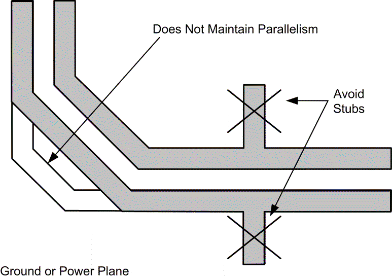
GUID-5B0FE4FE-5139-4638-8D54-C189B0F31EF6-low.pngFigure 12-1 Differential Signal Traces

Within the differential pairs, trace lengths must be run parallel to each other and be matched in length. Matched lengths minimize delay differences, avoiding an increase in common mode noise and emissions. Length matching is also important for MAC interface connections. All MII and RMII transmit signal traces should be length matched to each other and all MII and RMII receive signal traces should be length matched to each other.

Ideally, there should be no crossover or vias on signal path traces. Vias present impedance discontinuities and should be minimized when possible. Route trace pairs on the same layer. Signals on different layers should not cross each other without at least one return path plane between them. Differential pairs should always have a constant coupling distance between them. For convenience and efficiency, TI recommends routing critical signals first (that is, MDI differential pairs, reference clock, and MAC IF traces).