ZHCSAB9E September 2012 – June 2019 DP83848-EP
PRODUCTION DATA.
- 1 器件概述
- 2 修订历史记录
- 3 Pin Configuration and Functions
-
4 Specifications
- 4.1 Absolute Maximum Ratings
- 4.2 ESD Ratings
- 4.3 Recommended Operating Conditions
- 4.4 Thermal Information
- 4.5 DC Specifications
- 4.6
AC Specifications
- 4.6.1 Power Up Timing
- 4.6.2 Reset Timing
- 4.6.3 MII Serial Management Timing
- 4.6.4 100-Mbps MII Transmit Timing
- 4.6.5 100-Mbps MII Receive Timing
- 4.6.6 100BASE-TX Transmit Packet Latency Timing
- 4.6.7 100BASE-TX Transmit Packet Deassertion Timing
- 4.6.8 100BASE-TX Transmit Timing (tR/F and Jitter)
- 4.6.9 100BASE-TX Receive Packet Latency Timing
- 4.6.10 100BASE-TX Receive Packet Deassertion Timing
- 4.6.11 10-Mbps MII Transmit Timing
- 4.6.12 10-Mbps MII Receive Timing
- 4.6.13 10-Mbps Serial Mode Transmit Timing
- 4.6.14 10-Mbps Serial Mode Receive Timing
- 4.6.15 10BASE-T Transmit Timing (Start of Packet)
- 4.6.16 10BASE-T Transmit Timing (End of Packet)
- 4.6.17 10BASE-T Receive Timing (Start of Packet)
- 4.6.18 10BASE-T Receive Timing (End of Packet)
- 4.6.19 10-Mbps Heartbeat Timing
- 4.6.20 10-Mbps Jabber Timing
- 4.6.21 10BASE-T Normal Link Pulse Timing
- 4.6.22 Auto-Negotiation Fast Link Pulse (FLP) Timing
- 4.6.23 100BASE-TX Signal Detect Timing
- 4.6.24 100-Mbps Internal Loopback Timing
- 4.6.25 10-Mbps Internal Loopback Timing
- 4.6.26 RMII Transmit Timing
- 4.6.27 RMII Receive Timing
- 4.6.28 Isolation Timing
- 4.6.29 25MHz_OUT Timing
-
5 Detailed Description
- 5.1 Overview
- 5.2 Functional Block Diagram
- 5.3 Feature Description
- 5.4 Device Functional Modes
- 5.5
Programming
- 5.5.1
Architecture
- 5.5.1.1 100BASE-TX Transmitter
- 5.5.1.2
100BASE-TX Receiver
- 5.5.1.2.1 Analog Front End
- 5.5.1.2.2 Digital Signal Processor
- 5.5.1.2.3 Signal Detect
- 5.5.1.2.4 MLT-3 to NRZI Decoder
- 5.5.1.2.5 NRZI to NRZ
- 5.5.1.2.6 Serial to Parallel
- 5.5.1.2.7 Descrambler
- 5.5.1.2.8 Code-group Alignment
- 5.5.1.2.9 4B/5B Decoder
- 5.5.1.2.10 100BASE-TX Link Integrity Monitor
- 5.5.1.2.11 Bad SSD Detection
- 5.5.1.3
10BASE-T Transceiver Module
- 5.5.1.3.1 Operational Modes
- 5.5.1.3.2 Smart Squelch
- 5.5.1.3.3 Collision Detection and SQE
- 5.5.1.3.4 Carrier Sense
- 5.5.1.3.5 Normal Link Pulse Detection and Generation
- 5.5.1.3.6 Jabber Function
- 5.5.1.3.7 Automatic Link Polarity Detection and Correction
- 5.5.1.3.8 Transmit and Receive Filtering
- 5.5.1.3.9 Transmitter
- 5.5.1.3.10 Receiver
- 5.5.1
Architecture
- 5.6
Memory
- 5.6.1
Register Definition
- 5.6.1.1 Basic Mode Control Register (BMCR)
- 5.6.1.2 Basic Mode Status Register (BMSR)
- 5.6.1.3 PHY Identifier Register #1 (PHYIDR1)
- 5.6.1.4 PHY Identifier Register #2 (PHYIDR2)
- 5.6.1.5 Auto-Negotiation Advertisement Register (ANAR)
- 5.6.1.6 Auto-Negotiation Link Partner Ability Register (ANLPAR) (BASE Page)
- 5.6.1.7 Auto-Negotiation Link Partner Ability Register (ANLPAR) (Next Page)
- 5.6.1.8 Auto-Negotiate Expansion Register (ANER)
- 5.6.1.9 Auto-Negotiation Next Page Transmit Register (ANNPTR)
- 5.6.2
Extended Registers
- 5.6.2.1 PHY Status Register (PHYSTS)
- 5.6.2.2 MII Interrupt Control Register (MICR)
- 5.6.2.3 MII Interrupt Status and Miscellaneous Control Register (MISR)
- 5.6.2.4 False Carrier Sense Counter Register (FCSCR)
- 5.6.2.5 Receiver Error Counter Register (RECR)
- 5.6.2.6 100 Mbps PCS Configuration and Status Register (PCSR)
- 5.6.2.7 RMII and Bypass Register (RBR)
- 5.6.2.8 LED Direct Control Register (LEDCR)
- 5.6.2.9 PHY Control Register (PHYCR)
- 5.6.2.10 10Base-T Status/Control Register (10BTSCR)
- 5.6.2.11 CD Test and BIST Extensions Register (CDCTRL1)
- 5.6.2.12 Energy Detect Control (EDCR)
- 5.6.1
Register Definition
- 6 Application and Implementation
- 7 Power Supply Recommendations
- 8 Layout
- 9 器件和文档支持
- 10机械、封装和可订购信息
封装选项
机械数据 (封装 | 引脚)
散热焊盘机械数据 (封装 | 引脚)
订购信息
5.5.1.1 100BASE-TX Transmitter
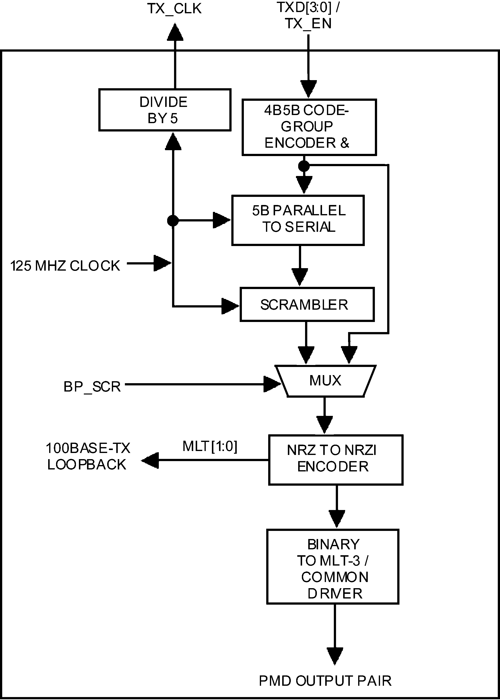
The 100BASE-TX transmitter consists of several functional blocks which convert synchronous 4-bit nibble data, as provided by the MII, to a scrambled MLT-3 125-Mbps serial data stream. Because the 100BASE-TX TP-PMD is integrated, the differential output pins, PMD Output Pair, can be directly routed to the magnetics. The block diagram in Figure 5-5 provides an overview of each functional block within the 100BASE-TX transmit section.
The Transmitter section consists of the following functional blocks:
- Code-group Encoder and Injection block
- Scrambler block (bypass option)
- NRZ to NRZI encoder block
- Binary to MLT-3 converter / Common Driver
The bypass option for the functional blocks within the 100BASE-TX transmitter provides flexibility for applications where data conversion is not always required. The DP83848-EP implements the 100BASE-TX transmit state machine diagram as specified in the IEEE 802.3u Standard, Clause 24.
 Figure 5-5 100BASE-TX Transmit Block Diagram
 Table 5-6 4B5B Code-Group Encoding/Decoding
| DATA CODES | ||
|---|---|---|
| 0 | 11110 | 0000 |
| 1 | 01001 | 0001 |
| 2 | 10100 | 0010 |
| 3 | 10101 | 0011 |
| 4 | 01010 | 0100 |
| 5 | 01011 | 0101 |
| 6 | 01110 | 0110 |
| 7 | 01111 | 0111 |
| 8 | 10010 | 1000 |
| 9 | 10011 | 1001 |
| A | 10110 | 1010 |
| B | 10111 | 1011 |
| C | 11010 | 1100 |
| D | 11011 | 1101 |
| E | 11100 | 1110 |
| F | 11101 | 1111 |
| IDLE AND CONTROL CODES | ||
| H | 00100 | HALT code-group - Error code |
| I | 11111 | Inter-Packet IDLE - 0000(1) |
| J | 11000 | First Start of Packet - 0101(1) |
| K | 10001 | Second Start of Packet - 0101(1) |
| T | 01101 | First End of Packet - 0000(1) |
| R | 00111 | Second End of Packet - 0000(1) |
| INVALID CODES | ||
| V | 00000 | |
| V | 00001 | |
| V | 00010 | |
| V | 00011 | |
| V | 00101 | |
| V | 00110 | |
| V | 01000 | |
| V | 01100 | |