ZHCSAB9E September 2012 – June 2019 DP83848-EP
PRODUCTION DATA.
- 1 器件概述
- 2 修订历史记录
- 3 Pin Configuration and Functions
-
4 Specifications
- 4.1 Absolute Maximum Ratings
- 4.2 ESD Ratings
- 4.3 Recommended Operating Conditions
- 4.4 Thermal Information
- 4.5 DC Specifications
- 4.6
AC Specifications
- 4.6.1 Power Up Timing
- 4.6.2 Reset Timing
- 4.6.3 MII Serial Management Timing
- 4.6.4 100-Mbps MII Transmit Timing
- 4.6.5 100-Mbps MII Receive Timing
- 4.6.6 100BASE-TX Transmit Packet Latency Timing
- 4.6.7 100BASE-TX Transmit Packet Deassertion Timing
- 4.6.8 100BASE-TX Transmit Timing (tR/F and Jitter)
- 4.6.9 100BASE-TX Receive Packet Latency Timing
- 4.6.10 100BASE-TX Receive Packet Deassertion Timing
- 4.6.11 10-Mbps MII Transmit Timing
- 4.6.12 10-Mbps MII Receive Timing
- 4.6.13 10-Mbps Serial Mode Transmit Timing
- 4.6.14 10-Mbps Serial Mode Receive Timing
- 4.6.15 10BASE-T Transmit Timing (Start of Packet)
- 4.6.16 10BASE-T Transmit Timing (End of Packet)
- 4.6.17 10BASE-T Receive Timing (Start of Packet)
- 4.6.18 10BASE-T Receive Timing (End of Packet)
- 4.6.19 10-Mbps Heartbeat Timing
- 4.6.20 10-Mbps Jabber Timing
- 4.6.21 10BASE-T Normal Link Pulse Timing
- 4.6.22 Auto-Negotiation Fast Link Pulse (FLP) Timing
- 4.6.23 100BASE-TX Signal Detect Timing
- 4.6.24 100-Mbps Internal Loopback Timing
- 4.6.25 10-Mbps Internal Loopback Timing
- 4.6.26 RMII Transmit Timing
- 4.6.27 RMII Receive Timing
- 4.6.28 Isolation Timing
- 4.6.29 25MHz_OUT Timing
-
5 Detailed Description
- 5.1 Overview
- 5.2 Functional Block Diagram
- 5.3 Feature Description
- 5.4 Device Functional Modes
- 5.5
Programming
- 5.5.1
Architecture
- 5.5.1.1 100BASE-TX Transmitter
- 5.5.1.2
100BASE-TX Receiver
- 5.5.1.2.1 Analog Front End
- 5.5.1.2.2 Digital Signal Processor
- 5.5.1.2.3 Signal Detect
- 5.5.1.2.4 MLT-3 to NRZI Decoder
- 5.5.1.2.5 NRZI to NRZ
- 5.5.1.2.6 Serial to Parallel
- 5.5.1.2.7 Descrambler
- 5.5.1.2.8 Code-group Alignment
- 5.5.1.2.9 4B/5B Decoder
- 5.5.1.2.10 100BASE-TX Link Integrity Monitor
- 5.5.1.2.11 Bad SSD Detection
- 5.5.1.3
10BASE-T Transceiver Module
- 5.5.1.3.1 Operational Modes
- 5.5.1.3.2 Smart Squelch
- 5.5.1.3.3 Collision Detection and SQE
- 5.5.1.3.4 Carrier Sense
- 5.5.1.3.5 Normal Link Pulse Detection and Generation
- 5.5.1.3.6 Jabber Function
- 5.5.1.3.7 Automatic Link Polarity Detection and Correction
- 5.5.1.3.8 Transmit and Receive Filtering
- 5.5.1.3.9 Transmitter
- 5.5.1.3.10 Receiver
- 5.5.1
Architecture
- 5.6
Memory
- 5.6.1
Register Definition
- 5.6.1.1 Basic Mode Control Register (BMCR)
- 5.6.1.2 Basic Mode Status Register (BMSR)
- 5.6.1.3 PHY Identifier Register #1 (PHYIDR1)
- 5.6.1.4 PHY Identifier Register #2 (PHYIDR2)
- 5.6.1.5 Auto-Negotiation Advertisement Register (ANAR)
- 5.6.1.6 Auto-Negotiation Link Partner Ability Register (ANLPAR) (BASE Page)
- 5.6.1.7 Auto-Negotiation Link Partner Ability Register (ANLPAR) (Next Page)
- 5.6.1.8 Auto-Negotiate Expansion Register (ANER)
- 5.6.1.9 Auto-Negotiation Next Page Transmit Register (ANNPTR)
- 5.6.2
Extended Registers
- 5.6.2.1 PHY Status Register (PHYSTS)
- 5.6.2.2 MII Interrupt Control Register (MICR)
- 5.6.2.3 MII Interrupt Status and Miscellaneous Control Register (MISR)
- 5.6.2.4 False Carrier Sense Counter Register (FCSCR)
- 5.6.2.5 Receiver Error Counter Register (RECR)
- 5.6.2.6 100 Mbps PCS Configuration and Status Register (PCSR)
- 5.6.2.7 RMII and Bypass Register (RBR)
- 5.6.2.8 LED Direct Control Register (LEDCR)
- 5.6.2.9 PHY Control Register (PHYCR)
- 5.6.2.10 10Base-T Status/Control Register (10BTSCR)
- 5.6.2.11 CD Test and BIST Extensions Register (CDCTRL1)
- 5.6.2.12 Energy Detect Control (EDCR)
- 5.6.1
Register Definition
- 6 Application and Implementation
- 7 Power Supply Recommendations
- 8 Layout
- 9 器件和文档支持
- 10机械、封装和可订购信息
封装选项
机械数据 (封装 | 引脚)
散热焊盘机械数据 (封装 | 引脚)
订购信息
5.5.1.2.2.2 Base Line Wander Compensation
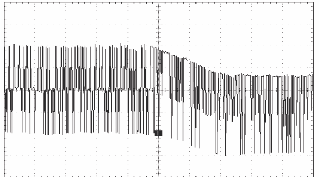
 Figure 5-8 100BASE-TX BLW Event
 The DP83848-EP is completely ANSI TP-PMD compliant and includes Base Line Wander (BLW) compensation. The BLW compensation block can successfully recover the TP-PMD defined “killer” pattern.
BLW can generally be defined as the change in the average DC content, relatively short period over time, of an AC coupled digital transmission over a given transmission medium. (that is, copper wire).
BLW results from the interaction between the low frequency components of a transmitted bit stream and the frequency response of the AC coupling component(s) within the transmission system. If the low frequency content of the digital bit stream goes below the low frequency pole of the AC coupling transformers then the droop characteristics of the transformers will dominate resulting in potentially serious BLW.
The digital oscilloscope plot provided in Figure 5-9 illustrates the severity of the BLW event that can theoretically be generated during 100BASE-TX packet transmission. This event consists of approximately 800 mV of DC offset for a period of 120 ms. Left uncompensated, events such as this can cause packet loss.