ZHCSEC3D October 2015 – November 2022 DP83867CS , DP83867E , DP83867IS
PRODUCTION DATA
- 1 特性
- 2 应用
- 3 说明
- 4 Revision History
- 5 Device Comparison
- 6 Pin Configuration and Functions
-
7 Specifications
- 7.1 Absolute Maximum Ratings
- 7.2 ESD Ratings
- 7.3 Recommended Operating Conditions
- 7.4 Thermal Information
- 7.5 Electrical Characteristics
- 7.6 Power-Up Timing
- 7.7 Reset Timing
- 7.8 MII Serial Management Timing
- 7.9 SGMII Timing
- 7.10 RGMII Timing
- 7.11 DP83867E Start of Frame Detection Timing
- 7.12 DP83867IS/CS Start of Frame Detection Timing
- 7.13 Timing Diagrams
- 7.14 Typical Characteristics
-
8 Detailed Description
- 8.1 Overview
- 8.2 Functional Block Diagram
- 8.3 Feature Description
- 8.4
Device Functional Modes
- 8.4.1 MAC Interfaces
- 8.4.2
Serial Management Interface
- 8.4.2.1
Extended Address Space Access
- 8.4.2.1.1 Write Address Operation
- 8.4.2.1.2 Read Address Operation
- 8.4.2.1.3 Write (No Post Increment) Operation
- 8.4.2.1.4 Read (No Post Increment) Operation
- 8.4.2.1.5 Write (Post Increment) Operation
- 8.4.2.1.6 Read (Post Increment) Operation
- 8.4.2.1.7 Example of Read Operation Using Indirect Register Access
- 8.4.2.1.8 Example of Write Operation Using Indirect Register Access
- 8.4.2.1
Extended Address Space Access
- 8.4.3
Auto-Negotiation
- 8.4.3.1 Speed and Duplex Selection - Priority Resolution
- 8.4.3.2 Master and Slave Resolution
- 8.4.3.3 Pause and Asymmetrical Pause Resolution
- 8.4.3.4 Next Page Support
- 8.4.3.5 Parallel Detection
- 8.4.3.6 Restart Auto-Negotiation
- 8.4.3.7 Enabling Auto-Negotiation Through Software
- 8.4.3.8 Auto-Negotiation Complete Time
- 8.4.3.9 Auto-MDIX Resolution
- 8.4.4 Loopback Mode
- 8.4.5 BIST Configuration
- 8.4.6 Cable Diagnostics
- 8.5 Programming
- 8.6
Register Maps
- 8.6.1 Basic Mode Control Register (BMCR)
- 8.6.2 Basic Mode Status Register (BMSR)
- 8.6.3 PHY Identifier Register #1 (PHYIDR1)
- 8.6.4 PHY Identifier Register #2 (PHYIDR2)
- 8.6.5 Auto-Negotiation Advertisement Register (ANAR)
- 8.6.6 Auto-Negotiation Link Partner Ability Register (ANLPAR) (BASE Page)
- 8.6.7 Auto-Negotiate Expansion Register (ANER)
- 8.6.8 Auto-Negotiation Next Page Transmit Register (ANNPTR)
- 8.6.9 Auto-Negotiation Next Page Receive Register (ANNPRR)
- 8.6.10 1000BASE-T Configuration Register (CFG1)
- 8.6.11 Status Register 1 (STS1)
- 8.6.12 Extended Register Addressing
- 8.6.13 1000BASE-T Status Register (1KSCR)
- 8.6.14 PHY Control Register (PHYCR)
- 8.6.15 PHY Status Register (PHYSTS)
- 8.6.16 MII Interrupt Control Register (MICR)
- 8.6.17 Interrupt Status Register (ISR)
- 8.6.18 Configuration Register 2 (CFG2)
- 8.6.19 Receiver Error Counter Register (RECR)
- 8.6.20 BIST Control Register (BISCR)
- 8.6.21 Status Register 2 (STS2)
- 8.6.22 LED Configuration Register 1 (LEDCR1)
- 8.6.23 LED Configuration Register 2 (LEDCR2)
- 8.6.24 LED Configuration Register (LEDCR3)
- 8.6.25 Configuration Register 3 (CFG3)
- 8.6.26 Control Register (CTRL)
- 8.6.27 Testmode Channel Control (TMCH_CTRL)
- 8.6.28 Robust Auto MDIX Timer Configuration Register (AMDIX_TMR_CFG)
- 8.6.29 Fast Link Drop Configuration Register (FLD_CFG)
- 8.6.30 Fast Link Drop Threshold Configuration Register (FLD_THR_CFG)
- 8.6.31 Configuration Register 4 (CFG4)
- 8.6.32 RGMII Control Register (RGMIICTL)
- 8.6.33 RGMII Control Register 2 (RGMIICTL2)
- 8.6.34 SGMII Auto-Negotiation Status (SGMII_ANEG_STS)
- 8.6.35 100BASE-TX Configuration (100CR)
- 8.6.36 Viterbi Module Configuration (VTM_CFG)
- 8.6.37 Skew FIFO Status (SKEW_FIFO)
- 8.6.38 Strap Configuration Status Register 1 (STRAP_STS1)
- 8.6.39 Strap Configuration Status Register 2 (STRAP_STS2)
- 8.6.40 BIST Control and Status Register 1 (BICSR1)
- 8.6.41 BIST Control and Status Register 2 (BICSR2)
- 8.6.42 BIST Control and Status Register 3 (BICSR3)
- 8.6.43 BIST Control and Status Register 4 (BICSR4)
- 8.6.44 Configuration for Receiver's Equalizer (CRE)
- 8.6.45 RGMII Delay Control Register (RGMIIDCTL)
- 8.6.46 Configuration of Receiver's LPF (CRLPF)
- 8.6.47 Enable Control of Receiver's Equalizer (ECRE)
- 8.6.48 PLL Clock-out Control Register (PLLCTL)
- 8.6.49 SGMII Control Register 1 (SGMIICTL1)
- 8.6.50 Sync FIFO Control (SYNC_FIFO_CTRL)
- 8.6.51 Loopback Configuration Register (LOOPCR)
- 8.6.52 DSP Configuration (DSP_CONFIG)
- 8.6.53 DSP Feedforward Equalizer Configuration (DSP_FFE_CFG)
- 8.6.54 Receive Configuration Register (RXFCFG)
- 8.6.55 Receive Status Register (RXFSTS)
- 8.6.56 Pattern Match Data Register 1 (RXFPMD1)
- 8.6.57 Pattern Match Data Register 2 (RXFPMD2)
- 8.6.58 Pattern Match Data Register 3 (RXFPMD3)
- 8.6.59 SecureOn Pass Register 2 (RXFSOP1)
- 8.6.60 SecureOn Pass Register 2 (RXFSOP2)
- 8.6.61 SecureOn Pass Register 3 (RXFSOP3)
- 8.6.62 Receive Pattern Register 1 (RXFPAT1)
- 8.6.63 Receive Pattern Register 2 (RXFPAT2)
- 8.6.64 Receive Pattern Register 3 (RXFPAT3)
- 8.6.65 Receive Pattern Register 4 (RXFPAT4)
- 8.6.66 Receive Pattern Register 5 (RXFPAT5)
- 8.6.67 Receive Pattern Register 6 (RXFPAT6)
- 8.6.68 Receive Pattern Register 7 (RXFPAT7)
- 8.6.69 Receive Pattern Register 8 (RXFPAT8)
- 8.6.70 Receive Pattern Register 9 (RXFPAT9)
- 8.6.71 Receive Pattern Register 10 (RXFPAT10)
- 8.6.72 Receive Pattern Register 11 (RXFPAT11)
- 8.6.73 Receive Pattern Register 12 (RXFPAT12)
- 8.6.74 Receive Pattern Register 13 (RXFPAT13)
- 8.6.75 Receive Pattern Register 14 (RXFPAT14)
- 8.6.76 Receive Pattern Register 15 (RXFPAT15)
- 8.6.77 Receive Pattern Register 16 (RXFPAT16)
- 8.6.78 Receive Pattern Register 17 (RXFPAT17)
- 8.6.79 Receive Pattern Register 18 (RXFPAT18)
- 8.6.80 Receive Pattern Register 19 (RXFPAT19)
- 8.6.81 Receive Pattern Register 20 (RXFPAT20)
- 8.6.82 Receive Pattern Register 21 (RXFPAT21)
- 8.6.83 Receive Pattern Register 22 (RXFPAT22)
- 8.6.84 Receive Pattern Register 23 (RXFPAT23)
- 8.6.85 Receive Pattern Register 24 (RXFPAT24)
- 8.6.86 Receive Pattern Register 25 (RXFPAT25)
- 8.6.87 Receive Pattern Register 26 (RXFPAT26)
- 8.6.88 Receive Pattern Register 27 (RXFPAT27)
- 8.6.89 Receive Pattern Register 28 (RXFPAT28)
- 8.6.90 Receive Pattern Register 29 (RXFPAT29)
- 8.6.91 Receive Pattern Register 30 (RXFPAT30)
- 8.6.92 Receive Pattern Register 31 (RXFPAT31)
- 8.6.93 Receive Pattern Register 32 (RXFPAT32)
- 8.6.94 Receive Pattern Byte Mask Register 1 (RXFPBM1)
- 8.6.95 Receive Pattern Byte Mask Register 2 (RXFPBM2)
- 8.6.96 Receive Pattern Byte Mask Register 3 (RXFPBM3)
- 8.6.97 Receive Pattern Byte Mask Register 4 (RXFPBM4)
- 8.6.98 Receive Pattern Control (RXFPATC)
- 8.6.99 10M SGMII Configuration (10M_SGMII_CFG)
- 8.6.100 I/O Configuration (IO_MUX_CFG)
- 8.6.101 GPIO Mux Control Register (GPIO_MUX_CTRL)
- 8.6.102 TDR General Configuration Register 1 (TDR_GEN_CFG1)
- 8.6.103 TDR Peak Locations Register 1 (TDR_PEAKS_LOC_1)
- 8.6.104 TDR Peak Locations Register 2 (TDR_PEAKS_LOC_2)
- 8.6.105 TDR Peak Locations Register 3 (TDR_PEAKS_LOC_3)
- 8.6.106 TDR Peak Locations Register 4 (TDR_PEAKS_LOC_4)
- 8.6.107 TDR Peak Locations Register 5 (TDR_PEAKS_LOC_5)
- 8.6.108 TDR Peak Locations Register 6 (TDR_PEAKS_LOC_6)
- 8.6.109 TDR Peak Locations Register 7 (TDR_PEAKS_LOC_7)
- 8.6.110 TDR Peak Locations Register 8 (TDR_PEAKS_LOC_8)
- 8.6.111 TDR Peak Locations Register 9 (TDR_PEAKS_LOC_9)
- 8.6.112 TDR Peak Locations Register 10 (TDR_PEAKS_LOC_10)
- 8.6.113 TDR Peak Amplitudes Register 1 (TDR_PEAKS_AMP_1)
- 8.6.114 TDR Peak Amplitudes Register 2 (TDR_PEAKS_AMP_2)
- 8.6.115 TDR Peak Amplitudes Register 3 (TDR_PEAKS_AMP_3)
- 8.6.116 TDR Peak Amplitudes Register 4 (TDR_PEAKS_AMP_4)
- 8.6.117 TDR Peak Amplitudes Register 5 (TDR_PEAKS_AMP_5)
- 8.6.118 TDR Peak Amplitudes Register 6 (TDR_PEAKS_AMP_6)
- 8.6.119 TDR Peak Amplitudes Register 7 (TDR_PEAKS_AMP_7)
- 8.6.120 TDR Peak Amplitudes Register 8 (TDR_PEAKS_AMP_8)
- 8.6.121 TDR Peak Amplitudes Register 9 (TDR_PEAKS_AMP_9)
- 8.6.122 TDR Peak Amplitudes Register 10 (TDR_PEAKS_AMP_10)
- 8.6.123 TDR General Status (TDR_GEN_STATUS)
- 8.6.124 Programmable Gain Register (PROG_GAIN)
- 8.6.125 MMD3 PCS Control Register (MMD3_PCS_CTRL)
- 9 Application and Implementation
- 10Power Supply Recommendations
- 11Layout
- 12Device and Documentation Support
封装选项
请参考 PDF 数据表获取器件具体的封装图。
机械数据 (封装 | 引脚)
- RGZ|48
散热焊盘机械数据 (封装 | 引脚)
- RGZ|48
订购信息
8.4.1.1 Serial GMII (SGMII)
The Serial Gigabit Media Independent Interface (SGMII) provides a means of conveying network data and port speed between a 100/1000 PHY and a MAC with significantly less signal pins (4 or 6 pins) than required for GMII (24 pins) or RGMII (12 pins). The SGMII interface uses 1.25-Gbps LVDS differential signaling which has the added benefit of reducing EMI emissions relative to GMII or RGMII.
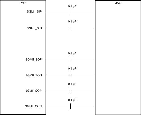
Because the internal clock and data recovery circuitry (CDR) of DP83867 can detect the transmit timing of the SGMII data, TX_CLK is not required. SGMII interface is capable of working as a 4-wire or 6-wire SGMII interface. The default SGMII connection is through four wires. Two differential pairs are used for the transmit and receive connections. Clock and data recovery are performed in the MAC and in the PHY, so no additional differential pair is required for clocking. Alternately, if the MAC is not capable of recovering the clock from the SGMII receive data, the DP83867 can be configured to provide the SGMII receive clock through a differential pair.
The 1.25-Gbps rate of SGMII is excessive for 100-Mbps operation. When operating in 100-Mbps mode, the PHY elongates the frame by replicating each frame byte 10 times. This frame elongation takes place above the IEEE 802.3 PCS layer, thus the start of frame delimiter only appears once per frame.
The SGMII interface includes Auto-Negotiation capability. Auto-Negotiation provides a mechanism for control information to be exchanged between the PHY and the MAC. This allows the interface to be automatically configured based on the media speed mode resolution on the MDI side. In MAC loopback mode, the SGMII speed is determined by the MDI speed selection. The SGMII interface works in both Auto-Negotiation and forced speed mode during the MAC loopback operation. SGMII Auto-Negotiation is the default mode of the operation.
The SGMII Auto-Negotiation process can be disabled and the SGMII speed mode can be forced to the MDI resolved speed. The SGMII forced speed mode can be enabled with the MDI auto-negotiation or MDI manual speed mode. SGMII Auto-Negotiation can be disabled through the SGMII_AUTONEG_EN register bit in the CFG2 register (address 0x0014).
The 10M_SGMII_RATE_ADAPT bit (bit 7) does not need to be changed for 10M speed as the PHY will automatically adapt the rate of SGMII.
SGMII is enabled through a resistor strap option. See Section 8.5.1 for details.
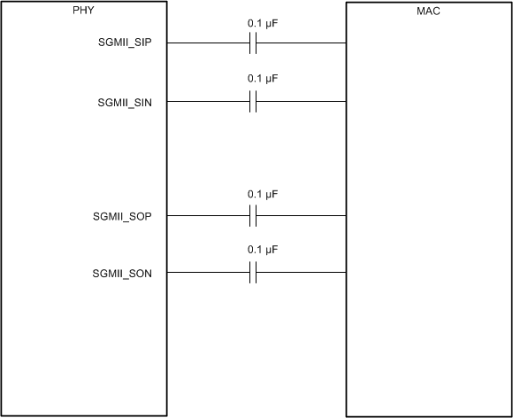
All SGMII connections must be AC-coupled through an 0.1-µF capacitor. PHY has inbuilt 100 Ω differential termination at receive and transmit pins of SGMII.
The connection diagrams for 4-wire SGMII and 6-wire SGMII are shown in Figure 8-4 and Figure 8-5.
 Figure 8-4 SGMII 4-Wire Connections
 Figure 8-5 SGMII 6-Wire Connections