ZHCSDE3G February 2015 – October 2022 DP83867CR , DP83867IR
PRODUCTION DATA
- 1 特性
- 2 应用
- 3 说明
- 4 Revision History
- 5 Device Comparison
- 6 Pin Configuration and Functions
-
7 Specifications
- 7.1 Absolute Maximum Ratings
- 7.2 ESD Ratings
- 7.3 Recommended Operating Conditions
- 7.4 Thermal Information
- 7.5 Electrical Characteristics
- 7.6 Power-Up Timing
- 7.7 Reset Timing
- 7.8 MII Serial Management Timing
- 7.9 RGMII Timing
- 7.10 GMII Transmit Timing (1)
- 7.11 GMII Receive Timing (1)
- 7.12 100-Mbps MII Transmit Timing (1)
- 7.13 100-Mbps MII Receive Timing (1)
- 7.14 10-Mbps MII Transmit Timing (1)
- 7.15 10-Mbps MII Receive Timing (1)
- 7.16 DP83867IR/CR Start of Frame Detection Timing
- 7.17 Timing Diagrams
- 7.18 Typical Characteristics
-
8 Detailed Description
- 8.1 Overview
- 8.2 Functional Block Diagram
- 8.3 Feature Description
- 8.4
Device Functional Modes
- 8.4.1 MAC Interfaces
- 8.4.2
Serial Management Interface
- 8.4.2.1
Extended Address Space Access
- 8.4.2.1.1 Write Address Operation
- 8.4.2.1.2 Read Address Operation
- 8.4.2.1.3 Write (No Post Increment) Operation
- 8.4.2.1.4 Read (No Post Increment) Operation
- 8.4.2.1.5 Write (Post Increment) Operation
- 8.4.2.1.6 Read (Post Increment) Operation
- 8.4.2.1.7 Example of Read Operation Using Indirect Register Access
- 8.4.2.1.8 Example of Write Operation Using Indirect Register Access
- 8.4.2.1
Extended Address Space Access
- 8.4.3
Auto-Negotiation
- 8.4.3.1 Speed and Duplex Selection - Priority Resolution
- 8.4.3.2 Master and Slave Resolution
- 8.4.3.3 Pause and Asymmetrical Pause Resolution
- 8.4.3.4 Next Page Support
- 8.4.3.5 Parallel Detection
- 8.4.3.6 Restart Auto-Negotiation
- 8.4.3.7 Enabling Auto-Negotiation Through Software
- 8.4.3.8 Auto-Negotiation Complete Time
- 8.4.3.9 Auto-MDIX Resolution
- 8.4.4 Loopback Mode
- 8.4.5 BIST Configuration
- 8.4.6 Cable Diagnostics
- 8.5 Programming
- 8.6
Register Maps
- 8.6.1 Basic Mode Control Register (BMCR)
- 8.6.2 Basic Mode Status Register (BMSR)
- 8.6.3 PHY Identifier Register #1 (PHYIDR1)
- 8.6.4 PHY Identifier Register #2 (PHYIDR2)
- 8.6.5 Auto-Negotiation Advertisement Register (ANAR)
- 8.6.6 Auto-Negotiation Link Partner Ability Register (ANLPAR) (BASE Page)
- 8.6.7 Auto-Negotiate Expansion Register (ANER)
- 8.6.8 Auto-Negotiation Next Page Transmit Register (ANNPTR)
- 8.6.9 Auto-Negotiation Next Page Receive Register (ANNPRR)
- 8.6.10 1000BASE-T Configuration Register (CFG1)
- 8.6.11 Status Register 1 (STS1)
- 8.6.12 Extended Register Addressing
- 8.6.13 1000BASE-T Status Register (1KSCR)
- 8.6.14 PHY Control Register (PHYCR)
- 8.6.15 PHY Status Register (PHYSTS)
- 8.6.16 MII Interrupt Control Register (MICR)
- 8.6.17 Interrupt Status Register (ISR)
- 8.6.18 Configuration Register 2 (CFG2)
- 8.6.19 Receiver Error Counter Register (RECR)
- 8.6.20 BIST Control Register (BISCR)
- 8.6.21 Status Register 2 (STS2)
- 8.6.22 LED Configuration Register 1 (LEDCR1)
- 8.6.23 LED Configuration Register 2 (LEDCR2)
- 8.6.24 LED Configuration Register (LEDCR3)
- 8.6.25 Configuration Register 3 (CFG3)
- 8.6.26 Control Register (CTRL)
- 8.6.27 Testmode Channel Control (TMCH_CTRL)
- 8.6.28 Robust Auto MDIX Timer Configuration Register (AMDIX_TMR_CFG)
- 8.6.29 Fast Link Drop Configuration Register (FLD_CFG)
- 8.6.30 Fast Link Drop Threshold Configuration Register (FLD_THR_CFG)
- 8.6.31 Configuration Register 4 (CFG4)
- 8.6.32 RGMII Control Register (RGMIICTL)
- 8.6.33 RGMII Control Register 2 (RGMIICTL2)
- 8.6.34 100BASE-TX Configuration (100CR)
- 8.6.35 Viterbi Module Configuration (VTM_CFG)
- 8.6.36 Skew FIFO Status (SKEW_FIFO)
- 8.6.37 Strap Configuration Status Register 1 (STRAP_STS1)
- 8.6.38 Strap Configuration Status Register 2 (STRAP_STS2)
- 8.6.39 BIST Control and Status Register 1 (BICSR1)
- 8.6.40 BIST Control and Status Register 2 (BICSR2)
- 8.6.41 BIST Control and Status Register 3 (BICSR3)
- 8.6.42 BIST Control and Status Register 4 (BICSR4)
- 8.6.43 Configuration for Receiver's Equalizer (CRE)
- 8.6.44 RGMII Delay Control Register (RGMIIDCTL)
- 8.6.45 Configuration of Receiver's LPF (CRLPF)
- 8.6.46 Enable Control of Receiver's Equalizer (ECRE)
- 8.6.47 PLL Clock-out Control Register (PLLCTL)
- 8.6.48 Sync FIFO Control (SYNC_FIFO_CTRL)
- 8.6.49 Loopback Configuration Register (LOOPCR)
- 8.6.50 DSP Configuration (DSP_CONFIG)
- 8.6.51 DSP Feedforward Equalizer Configuration (DSP_FFE_CFG)
- 8.6.52 Receive Configuration Register (RXFCFG)
- 8.6.53 Receive Status Register (RXFSTS)
- 8.6.54 Pattern Match Data Register 1 (RXFPMD1)
- 8.6.55 Pattern Match Data Register 2 (RXFPMD2)
- 8.6.56 Pattern Match Data Register 3 (RXFPMD3)
- 8.6.57 SecureOn Pass Register 2 (RXFSOP1)
- 8.6.58 SecureOn Pass Register 2 (RXFSOP2)
- 8.6.59 SecureOn Pass Register 3 (RXFSOP3)
- 8.6.60 Receive Pattern Register 1 (RXFPAT1)
- 8.6.61 Receive Pattern Register 2 (RXFPAT2)
- 8.6.62 Receive Pattern Register 3 (RXFPAT3)
- 8.6.63 Receive Pattern Register 4 (RXFPAT4)
- 8.6.64 Receive Pattern Register 5 (RXFPAT5)
- 8.6.65 Receive Pattern Register 6 (RXFPAT6)
- 8.6.66 Receive Pattern Register 7 (RXFPAT7)
- 8.6.67 Receive Pattern Register 8 (RXFPAT8)
- 8.6.68 Receive Pattern Register 9 (RXFPAT9)
- 8.6.69 Receive Pattern Register 10 (RXFPAT10)
- 8.6.70 Receive Pattern Register 11 (RXFPAT11)
- 8.6.71 Receive Pattern Register 12 (RXFPAT12)
- 8.6.72 Receive Pattern Register 13 (RXFPAT13)
- 8.6.73 Receive Pattern Register 14 (RXFPAT14)
- 8.6.74 Receive Pattern Register 15 (RXFPAT15)
- 8.6.75 Receive Pattern Register 16 (RXFPAT16)
- 8.6.76 Receive Pattern Register 17 (RXFPAT17)
- 8.6.77 Receive Pattern Register 18 (RXFPAT18)
- 8.6.78 Receive Pattern Register 19 (RXFPAT19)
- 8.6.79 Receive Pattern Register 20 (RXFPAT20)
- 8.6.80 Receive Pattern Register 21 (RXFPAT21)
- 8.6.81 Receive Pattern Register 22 (RXFPAT22)
- 8.6.82 Receive Pattern Register 23 (RXFPAT23)
- 8.6.83 Receive Pattern Register 24 (RXFPAT24)
- 8.6.84 Receive Pattern Register 25 (RXFPAT25)
- 8.6.85 Receive Pattern Register 26 (RXFPAT26)
- 8.6.86 Receive Pattern Register 27 (RXFPAT27)
- 8.6.87 Receive Pattern Register 28 (RXFPAT28)
- 8.6.88 Receive Pattern Register 29 (RXFPAT29)
- 8.6.89 Receive Pattern Register 30 (RXFPAT30)
- 8.6.90 Receive Pattern Register 31 (RXFPAT31)
- 8.6.91 Receive Pattern Register 32 (RXFPAT32)
- 8.6.92 Receive Pattern Byte Mask Register 1 (RXFPBM1)
- 8.6.93 Receive Pattern Byte Mask Register 2 (RXFPBM2)
- 8.6.94 Receive Pattern Byte Mask Register 3 (RXFPBM3)
- 8.6.95 Receive Pattern Byte Mask Register 4 (RXFPBM4)
- 8.6.96 Receive Pattern Control (RXFPATC)
- 8.6.97 I/O Configuration (IO_MUX_CFG)
- 8.6.98 GPIO Mux Control Register 1 (GPIO_MUX_CTRL1)
- 8.6.99 GPIO Mux Control Register 2 (GPIO_MUX_CTRL2)
- 8.6.100 GPIO Mux Control Register (GPIO_MUX_CTRL)
- 8.6.101 TDR General Configuration Register 1 (TDR_GEN_CFG1)
- 8.6.102 TDR Peak Locations Register 1 (TDR_PEAKS_LOC_1)
- 8.6.103 TDR Peak Locations Register 2 (TDR_PEAKS_LOC_2)
- 8.6.104 TDR Peak Locations Register 3 (TDR_PEAKS_LOC_3)
- 8.6.105 TDR Peak Locations Register 4 (TDR_PEAKS_LOC_4)
- 8.6.106 TDR Peak Locations Register 5 (TDR_PEAKS_LOC_5)
- 8.6.107 TDR Peak Locations Register 6 (TDR_PEAKS_LOC_6)
- 8.6.108 TDR Peak Locations Register 7 (TDR_PEAKS_LOC_7)
- 8.6.109 TDR Peak Locations Register 8 (TDR_PEAKS_LOC_8)
- 8.6.110 TDR Peak Locations Register 9 (TDR_PEAKS_LOC_9)
- 8.6.111 TDR Peak Locations Register 10 (TDR_PEAKS_LOC_10)
- 8.6.112 TDR Peak Amplitudes Register 1 (TDR_PEAKS_AMP_1)
- 8.6.113 TDR Peak Amplitudes Register 2 (TDR_PEAKS_AMP_2)
- 8.6.114 TDR Peak Amplitudes Register 3 (TDR_PEAKS_AMP_3)
- 8.6.115 TDR Peak Amplitudes Register 4 (TDR_PEAKS_AMP_4)
- 8.6.116 TDR Peak Amplitudes Register 5 (TDR_PEAKS_AMP_5)
- 8.6.117 TDR Peak Amplitudes Register 6 (TDR_PEAKS_AMP_6)
- 8.6.118 TDR Peak Amplitudes Register 7 (TDR_PEAKS_AMP_7)
- 8.6.119 TDR Peak Amplitudes Register 8 (TDR_PEAKS_AMP_8)
- 8.6.120 TDR Peak Amplitudes Register 9 (TDR_PEAKS_AMP_9)
- 8.6.121 TDR Peak Amplitudes Register 10 (TDR_PEAKS_AMP_10)
- 8.6.122 TDR General Status (TDR_GEN_STATUS)
- 9 Application and Implementation
- 10Power Supply Recommendations
- 11Layout
- 12Device and Documentation Support
封装选项
请参考 PDF 数据表获取器件具体的封装图。
机械数据 (封装 | 引脚)
- RGZ|48
- PAP|64
散热焊盘机械数据 (封装 | 引脚)
订购信息
10 Power Supply Recommendations
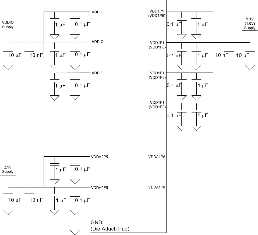
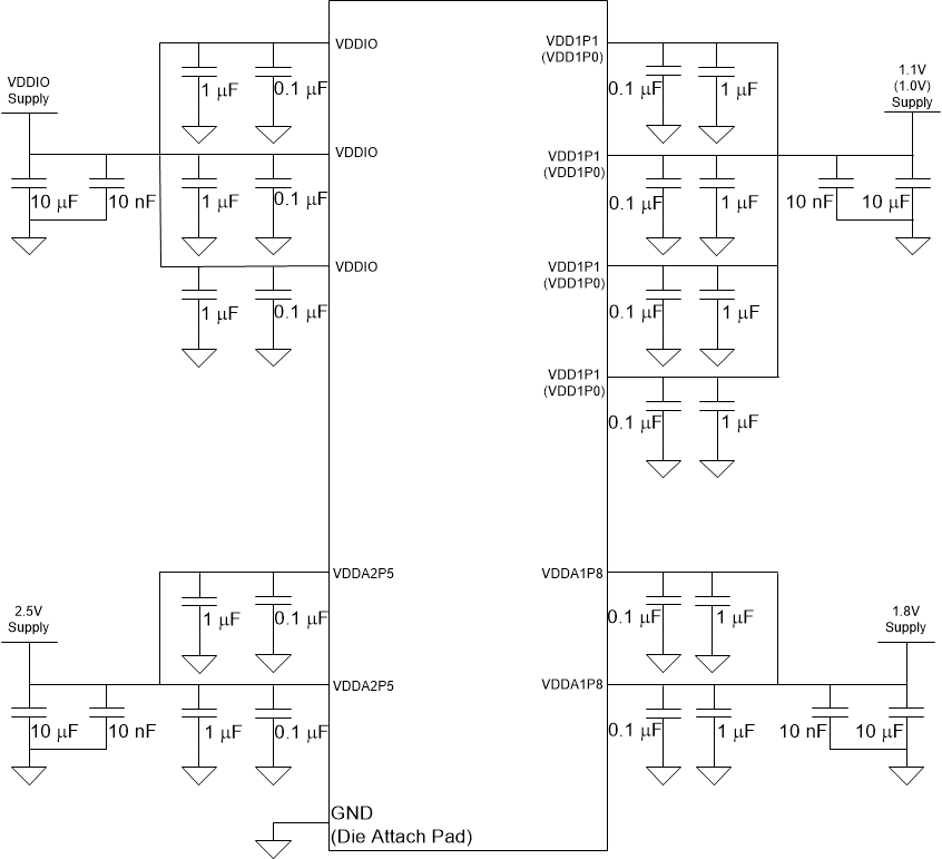
The DP83867 is capable of operating with as few as two or three supplies. The I/O power supply can also be operated independently of the main device power supplies to provide flexibility for the MAC interface.
For detailed information about DP83867 power consumption for specific supplies under a wide set of conditions, see the DP83867E/IS/CS/IR/CR RGZ Power Consumption Data application report (SNLA241).
The connection diagrams for the two-supply and three-supply configurations are shown in Figure 10-1 and Figure 10-2.


There is no requirement for the sequence of the supplies when operating in two-supply mode.
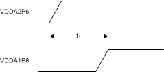
When operating in three-supply mode, the 1.8-V VDDA1P8 supply must be stable within 25 ms of the 2.5-V VDDA2P5 supply ramping up. There is no sequencing requirement for other supplies when operating in three-supply mode.
When powering down the DP83867, the 1.8-V supply should be brought down before the 2.5-V supply.
 Figure 10-3 Three-Supply Mode
Power Supply Sequence Diagram
Figure 10-3 Three-Supply Mode
Power Supply Sequence Diagram| PARAMETER | TEST CONDITIONS | MIN | NOM | MAX | UNIT | |
|---|---|---|---|---|---|---|
| T1 | Beginning of VDDA2P5 ramp up to VDDA1P8 stable | 0 | 25 | ms | ||
If the 2.5-V power supply provides power to DP83867 devices only, the 1.8-V supply may ramp up any time before 2.5-V.