ZHCSIS3C September 2018 – April 2024 DP83869HM
PRODUCTION DATA
- 1
- 1 特性
- 2 应用
- 3 说明
- 4 Device Comparison
- 5 Pin Configuration and Functions
- 6 Specifications
-
7 Detailed Description
- 7.1 Overview
- 7.2 Functional Block Diagram
- 7.3
Feature Description
- 7.3.1 WoL (Wake-on-LAN) Packet Detection
- 7.3.2 Start of Frame Detect for IEEE 1588 Time Stamp
- 7.3.3 Clock Output
- 7.3.4 Loopback Mode
- 7.3.5 BIST Configuration
- 7.3.6 Interrupt
- 7.3.7 Power-Saving Modes
- 7.3.8 Mirror Mode
- 7.3.9 Speed Optimization
- 7.3.10 Cable Diagnostics
- 7.3.11 Fast Link Drop
- 7.3.12 Jumbo Frames
- 7.4
Device Functional Modes
- 7.4.1 Copper Ethernet
- 7.4.2 Fiber Ethernet
- 7.4.3 Serial GMII (SGMII)
- 7.4.4 Reduced GMII (RGMII)
- 7.4.5 Media Independent Interface (MII)
- 7.4.6 Bridge Modes
- 7.4.7 Media Convertor Mode
- 7.4.8 Register Configuration for Operational Modes
- 7.4.9 Serial Management Interface
- 7.4.10
Auto-Negotiation
- 7.4.10.1 Speed and Duplex Selection - Priority Resolution
- 7.4.10.2 Master and Slave Resolution
- 7.4.10.3 Pause and Asymmetrical Pause Resolution
- 7.4.10.4 Next Page Support
- 7.4.10.5 Parallel Detection
- 7.4.10.6 Restart Auto-Negotiation
- 7.4.10.7 Enabling Auto-Negotiation Through Software
- 7.4.10.8 Auto-Negotiation Complete Time
- 7.4.10.9 Auto-MDIX Resolution
- 7.5
Programming
- 7.5.1
Strap Configuration
- 7.5.1.1 Straps for PHY Address
- 7.5.1.2 Strap for DP83869HM Functional Mode Selection
- 7.5.1.3 LED Default Configuration Based on Device Mode
- 7.5.1.4 Straps for RGMII/SGMII to Copper
- 7.5.1.5 Straps for RGMII to 1000Base-X
- 7.5.1.6 Straps for RGMII to 100Base-FX
- 7.5.1.7 Straps for Bridge Mode (SGMII-RGMII)
- 7.5.1.8 Straps for 100M Media Convertor
- 7.5.1.9 Straps for 1000M Media Convertor
- 7.5.2 LED Configuration
- 7.5.3 Reset Operation
- 7.5.1
Strap Configuration
- 7.6 Register Maps
- 8 Application and Implementation
- 9 Device and Documentation Support
- 10Revision History
- 11Mechanical, Packaging, and Orderable Information
7.4.3 Serial GMII (SGMII)
The Serial Gigabit Media Independent Interface (SGMII) provides a means of conveying network data and port speed between a 100/1000 PHY and a MAC with significantly less signal pins (4 or 6 pins) than required for GMII (24 pins) or RGMII (12 pins). The SGMII interface uses 1.25Gbps LVDS differential signaling which has the added benefit of reducing EMI emissions relative to GMII or RGMII.
Because the internal clock and data recovery circuitry (CDR) of DP83869HM can detect the transmit timing of the SGMII data, TX_CLK is not required. The DP83869HM supports only 4-wire SGMII mode. Two differential pairs are used for the transmit and receive connections. Clock and data recovery are performed in the MAC and in the PHY, so no additional differential pair is required for clocking.
The 1.25Gbps rate of SGMII is excessive for 100Mbps and 10Mbps operation. When operating in 100Mbps mode, the PHY elongates the frame by replicating each frame byte 10 times and when in 10Mbps mode the PHY elongates the frame by replicating each frame byte 100 times. This frame elongation takes place above the IEEE 802.3 PCS layer, thus the start of frame delimiter only appears once per frame.
The SGMII interface includes Auto-Negotiation capability. Auto-Negotiation provides a mechanism for control information to be exchanged between the PHY and the MAC. This allows the interface to be automatically configured based on the media speed mode resolution on the MDI side. In MAC loopback mode, the SGMII speed is determined by the MDI speed selection. The SGMII interface works in both Auto-Negotiation and forced speed mode during the MAC loopback operation. SGMII Auto-Negotiation is the default mode of the operation.
The SGMII Auto-Negotiation process can be disabled and the SGMII speed mode can be forced to the MDI resolved speed. The SGMII forced speed mode can be enabled with the MDI auto-negotiation or MDI manual speed mode. SGMII Auto-Negotiation can be disabled through the SGMII_AUTONEG_EN register bit in the CFG2 register (address 14h).
The 10M_SGMII_RATE_ADAPT bit (bit 7) of 10M_SGMII_CFG register (16Fh) needs to be cleared for enabling 10M SGMII operation.
SGMII is enabled through a resistor strap option. See Section 7.5.1 for details.
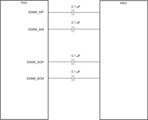
All SGMII connections must be AC-coupled through an 0.1µF capacitor.
The connection diagrams for 4-wire SGMII is shown in Figure 7-6.
MII Isolate (bit 10 in register 0h) does not isolate SGMII pins. SGMII can be disabled through register 1DFh for isolating SGMII pins.
 Figure 7-6 SGMII 4-Wire Connections