ZHCSQL1 May   2022 DP83TC813R-Q1 , DP83TC813S-Q1

PRODUCTION DATA  

  1. 特性
  2. 应用
  3. 说明
  4. Revision History
  5. Device Comparison Table
  6. Pin Configuration and Functions
  7. Specifications
    1. 7.1 Absolute Maximum Ratings
    2. 7.2 ESD Ratings
    3. 7.3 Recommended Operating Conditions
    4. 7.4 Thermal Information
    5. 7.5 Electrical Characteristics
    6. 7.6 Timing Requirements
    7. 7.7 Timing Diagrams
    8. 7.8 Typical Characteristics
  8. Detailed Description
    1. 8.1 Overview
    2. 8.2 Functional Block Diagram
    3. 8.3 Feature Description
      1. 8.3.1 Diagnostic Tool Kit
        1. 8.3.1.1 Signal Quality Indicator
        2. 8.3.1.2 Electrostatic Discharge Sensing
        3. 8.3.1.3 Time Domain Reflectometry
        4. 8.3.1.4 Voltage Sensing
        5. 8.3.1.5 BIST and Loopback Modes
          1. 8.3.1.5.1 Data Generator and Checker
          2. 8.3.1.5.2 xMII Loopback
          3. 8.3.1.5.3 PCS Loopback
          4. 8.3.1.5.4 Digital Loopback
          5. 8.3.1.5.5 Analog Loopback
          6. 8.3.1.5.6 Reverse Loopback
      2. 8.3.2 Compliance Test Modes
        1. 8.3.2.1 Test Mode 1
        2. 8.3.2.2 Test Mode 2
        3. 8.3.2.3 Test Mode 4
        4. 8.3.2.4 Test Mode 5
    4. 8.4 Device Functional Modes
      1. 8.4.1  Power Down
      2. 8.4.2  Reset
      3. 8.4.3  Standby
      4. 8.4.4  Normal
      5. 8.4.5  Sleep Ack
      6. 8.4.6  Sleep Request
      7. 8.4.7  Sleep Fail
      8. 8.4.8  Sleep
      9. 8.4.9  Wake-Up
      10. 8.4.10 TC10 System Example
      11. 8.4.11 Media Dependent Interface
        1. 8.4.11.1 100BASE-T1 Master and 100BASE-T1 Slave Configuration
        2. 8.4.11.2 Auto-Polarity Detection and Correction
        3. 8.4.11.3 Jabber Detection
        4. 8.4.11.4 Interleave Detection
      12. 8.4.12 MAC Interfaces
        1. 8.4.12.1 Media Independent Interface
        2. 8.4.12.2 Reduced Media Independent Interface
        3. 8.4.12.3 Reduced Gigabit Media Independent Interface
        4. 8.4.12.4 Serial Gigabit Media Independent Interface
      13. 8.4.13 Serial Management Interface
      14. 8.4.14 Direct Register Access
      15. 8.4.15 Extended Register Space Access
      16. 8.4.16 Write Address Operation
        1. 8.4.16.1 MMD1 - Write Address Operation
      17. 8.4.17 Read Address Operation
        1. 8.4.17.1 MMD1 - Read Address Operation
      18. 8.4.18 Write Operation (No Post Increment)
        1. 8.4.18.1 MMD1 - Write Operation (No Post Increment)
      19. 8.4.19 Read Operation (No Post Increment)
        1. 8.4.19.1 MMD1 - Read Operation (No Post Increment)
      20. 8.4.20 Write Operation (Post Increment)
        1. 8.4.20.1 MMD1 - Write Operation (Post Increment)
      21. 8.4.21 Read Operation (Post Increment)
        1. 8.4.21.1 MMD1 - Read Operation (Post Increment)
    5. 8.5 Programming
      1. 8.5.1 Strap Configuration
      2. 8.5.2 LED Configuration
      3. 8.5.3 PHY Address Configuration
    6. 8.6 Register Maps
      1. 8.6.1 Register Access Summary
      2. 8.6.2 DP83TC813 Registers
  9. Application and Implementation
    1. 9.1 Application Information
    2. 9.2 Typical Applications
      1. 9.2.1 Design Requirements
        1. 9.2.1.1 Physical Medium Attachment
          1. 9.2.1.1.1 Common-Mode Choke Recommendations
      2. 9.2.2 Detailed Design Procedure
      3. 9.2.3 Application Curves
  10. 10Power Supply Recommendations
  11. 11Layout
    1. 11.1 Layout Guidelines
      1. 11.1.1 Signal Traces
      2. 11.1.2 Return Path
      3. 11.1.3 Metal Pour
      4. 11.1.4 PCB Layer Stacking
    2. 11.2 Layout Example
  12. 12Device and Documentation Support
    1. 12.1 Receiving Notification of Documentation Updates
    2. 12.2 支持资源
    3. 12.3 Community Resources
    4. 12.4 Trademarks
    5. 12.5 Electrostatic Discharge Caution
    6. 12.6 术语表
  13. 13Mechanical, Packaging, and Orderable Information

封装选项

机械数据 (封装 | 引脚)
散热焊盘机械数据 (封装 | 引脚)
订购信息

PCB Layer Stacking

To meet signal integrity and performance requirements, minimum four-layer PCB is recommended. However, a six-layer PCB and above must be used when possible.
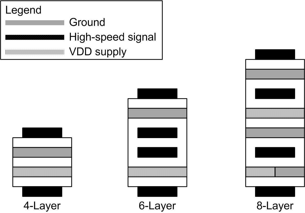
GUID-670E736E-484C-4EEA-9443-393BCB24FDEF-low.png Figure 11-3 Recommended PCB Layer Stack-Up