ZHCSQL1 May   2022 DP83TC813R-Q1 , DP83TC813S-Q1

PRODUCTION DATA  

  1. 特性
  2. 应用
  3. 说明
  4. Revision History
  5. Device Comparison Table
  6. Pin Configuration and Functions
  7. Specifications
    1. 7.1 Absolute Maximum Ratings
    2. 7.2 ESD Ratings
    3. 7.3 Recommended Operating Conditions
    4. 7.4 Thermal Information
    5. 7.5 Electrical Characteristics
    6. 7.6 Timing Requirements
    7. 7.7 Timing Diagrams
    8. 7.8 Typical Characteristics
  8. Detailed Description
    1. 8.1 Overview
    2. 8.2 Functional Block Diagram
    3. 8.3 Feature Description
      1. 8.3.1 Diagnostic Tool Kit
        1. 8.3.1.1 Signal Quality Indicator
        2. 8.3.1.2 Electrostatic Discharge Sensing
        3. 8.3.1.3 Time Domain Reflectometry
        4. 8.3.1.4 Voltage Sensing
        5. 8.3.1.5 BIST and Loopback Modes
          1. 8.3.1.5.1 Data Generator and Checker
          2. 8.3.1.5.2 xMII Loopback
          3. 8.3.1.5.3 PCS Loopback
          4. 8.3.1.5.4 Digital Loopback
          5. 8.3.1.5.5 Analog Loopback
          6. 8.3.1.5.6 Reverse Loopback
      2. 8.3.2 Compliance Test Modes
        1. 8.3.2.1 Test Mode 1
        2. 8.3.2.2 Test Mode 2
        3. 8.3.2.3 Test Mode 4
        4. 8.3.2.4 Test Mode 5
    4. 8.4 Device Functional Modes
      1. 8.4.1  Power Down
      2. 8.4.2  Reset
      3. 8.4.3  Standby
      4. 8.4.4  Normal
      5. 8.4.5  Sleep Ack
      6. 8.4.6  Sleep Request
      7. 8.4.7  Sleep Fail
      8. 8.4.8  Sleep
      9. 8.4.9  Wake-Up
      10. 8.4.10 TC10 System Example
      11. 8.4.11 Media Dependent Interface
        1. 8.4.11.1 100BASE-T1 Master and 100BASE-T1 Slave Configuration
        2. 8.4.11.2 Auto-Polarity Detection and Correction
        3. 8.4.11.3 Jabber Detection
        4. 8.4.11.4 Interleave Detection
      12. 8.4.12 MAC Interfaces
        1. 8.4.12.1 Media Independent Interface
        2. 8.4.12.2 Reduced Media Independent Interface
        3. 8.4.12.3 Reduced Gigabit Media Independent Interface
        4. 8.4.12.4 Serial Gigabit Media Independent Interface
      13. 8.4.13 Serial Management Interface
      14. 8.4.14 Direct Register Access
      15. 8.4.15 Extended Register Space Access
      16. 8.4.16 Write Address Operation
        1. 8.4.16.1 MMD1 - Write Address Operation
      17. 8.4.17 Read Address Operation
        1. 8.4.17.1 MMD1 - Read Address Operation
      18. 8.4.18 Write Operation (No Post Increment)
        1. 8.4.18.1 MMD1 - Write Operation (No Post Increment)
      19. 8.4.19 Read Operation (No Post Increment)
        1. 8.4.19.1 MMD1 - Read Operation (No Post Increment)
      20. 8.4.20 Write Operation (Post Increment)
        1. 8.4.20.1 MMD1 - Write Operation (Post Increment)
      21. 8.4.21 Read Operation (Post Increment)
        1. 8.4.21.1 MMD1 - Read Operation (Post Increment)
    5. 8.5 Programming
      1. 8.5.1 Strap Configuration
      2. 8.5.2 LED Configuration
      3. 8.5.3 PHY Address Configuration
    6. 8.6 Register Maps
      1. 8.6.1 Register Access Summary
      2. 8.6.2 DP83TC813 Registers
  9. Application and Implementation
    1. 9.1 Application Information
    2. 9.2 Typical Applications
      1. 9.2.1 Design Requirements
        1. 9.2.1.1 Physical Medium Attachment
          1. 9.2.1.1.1 Common-Mode Choke Recommendations
      2. 9.2.2 Detailed Design Procedure
      3. 9.2.3 Application Curves
  10. 10Power Supply Recommendations
  11. 11Layout
    1. 11.1 Layout Guidelines
      1. 11.1.1 Signal Traces
      2. 11.1.2 Return Path
      3. 11.1.3 Metal Pour
      4. 11.1.4 PCB Layer Stacking
    2. 11.2 Layout Example
  12. 12Device and Documentation Support
    1. 12.1 Receiving Notification of Documentation Updates
    2. 12.2 支持资源
    3. 12.3 Community Resources
    4. 12.4 Trademarks
    5. 12.5 Electrostatic Discharge Caution
    6. 12.6 术语表
  13. 13Mechanical, Packaging, and Orderable Information

封装选项

机械数据 (封装 | 引脚)
散热焊盘机械数据 (封装 | 引脚)
订购信息

LED Configuration

The DP83TC813S-Q1 supports 1 configurable LED pin (LED_1) which also doubles up as a clock output pin (CLKOUT). Several functions can be multiplexed onto the LEDs for different modes of operation. LED operations are selected using registers 0x0450.

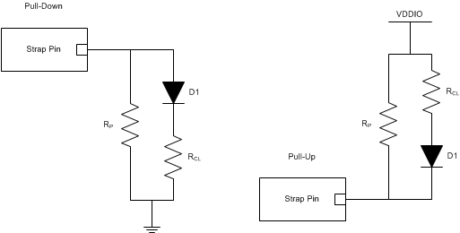
Because the LED output pins are also used as strap pins, external components required for strapping and the user must consider the LED usage to avoid contention. Specifically, when the LED outputs are used to drive LEDs directly, the active state of each output driver is dependent on the logic level sampled by the corresponding input upon power up or hardware reset.

Figure 8-19 shows the two proper ways of connecting LEDs directly to the DP83TC813S-Q1 .
GUID-9E0ABB78-76F3-414E-8E27-8F88BEE9D6AB-low.gifFigure 8-19 Example Strap Connections