ZHCSQL1 May 2022 DP83TC813R-Q1 , DP83TC813S-Q1
PRODUCTION DATA
- 1 特性
- 2 应用
- 3 说明
- 4 Revision History
- 5 Device Comparison Table
- 6 Pin Configuration and Functions
- 7 Specifications
-
8 Detailed Description
- 8.1 Overview
- 8.2 Functional Block Diagram
- 8.3 Feature Description
- 8.4
Device Functional Modes
- 8.4.1 Power Down
- 8.4.2 Reset
- 8.4.3 Standby
- 8.4.4 Normal
- 8.4.5 Sleep Ack
- 8.4.6 Sleep Request
- 8.4.7 Sleep Fail
- 8.4.8 Sleep
- 8.4.9 Wake-Up
- 8.4.10 TC10 System Example
- 8.4.11 Media Dependent Interface
- 8.4.12 MAC Interfaces
- 8.4.13 Serial Management Interface
- 8.4.14 Direct Register Access
- 8.4.15 Extended Register Space Access
- 8.4.16 Write Address Operation
- 8.4.17 Read Address Operation
- 8.4.18 Write Operation (No Post Increment)
- 8.4.19 Read Operation (No Post Increment)
- 8.4.20 Write Operation (Post Increment)
- 8.4.21 Read Operation (Post Increment)
- 8.5 Programming
- 8.6 Register Maps
- 9 Application and Implementation
- 10Power Supply Recommendations
- 11Layout
- 12Device and Documentation Support
- 13Mechanical, Packaging, and Orderable Information
8.4.12.3 Reduced Gigabit Media Independent Interface
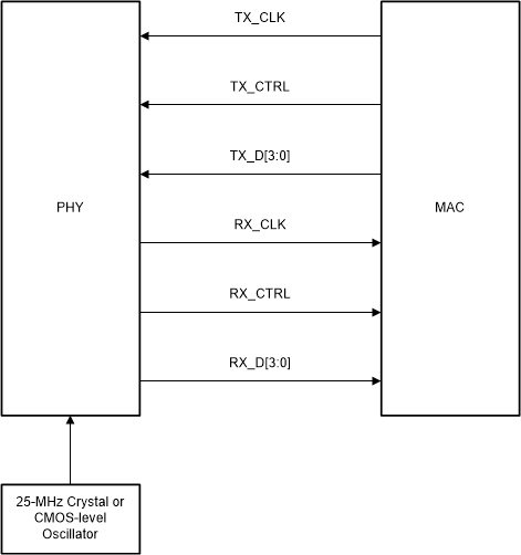
The DP83TC813-Q1 also supports Reduced Gigabit Media Independent Interface (RGMII) as specified by RGMII version 2.0 with LVCMOS. RGMII is designed to reduce the number of pins required to connect MAC and PHY. To accomplish this goal, the control signals are multiplexed. Both rising and falling edges of the clock are used to sample the control signal pin on transmit and receive paths. Data is samples on just the rising edge of the clock. For 100-Mbps operation, RX_CLK and TX_CLK operate at 25 MHz.
The RGMII signals are summarized in Table 8-10:
| FUNCTION | PINS |
|---|---|
| Data Signals | TX_D[3:0] |
| RX_D[3:0] | |
| Control Signals | TX_CTRL |
| RX_CTRL | |
| Clock Signals | TX_CLK |
| RX_CLK |
 Figure 8-16 RGMII Connections
| TX_CTRL (POSITIVE EDGE) | TX_CTRL (NEGATIVE EDGE) | TX_D[3:0] | DESCRIPTION |
|---|---|---|---|
| 0 | 0 | 0000 through 1111 | Normal Inter-Frame |
| 0 | 1 | 0000 through 1111 | Reserved |
| 1 | 0 | 0000 through 1111 | Normal Data Transmission |
| 1 | 1 | 0000 through 1111 | Transmit Error Propagation |
| RX_CTRL (POSITIVE EDGE) | RX_CTRL (NEGATIVE EDGE) | RX_D[3:0] | DESCRIPTION |
|---|---|---|---|
| 0 | 0 | 0000 through 1111 | Normal Inter-Frame |
| 0 | 1 | 0000 through 1101 | Reserved |
| 0 | 1 | 1110 | False Carrier Indication |
| 0 | 1 | 1111 | Reserved |
| 1 | 0 | 0000 through 1111 | Normal Data Reception |
| 1 | 1 | 0000 through 1111 | Data Reception with Errors |
During packet reception, RX_CLK may be stretched on either the positive or negative pulse to accommodate the transition from the internal free running clock to a recovered clock (data synchronous). Data may be duplicated on the falling edge of the clock because double data rate (DDR) is only required for 1-Gbps operation, which is not supported by the DP83TC813-Q1.
The DP83TC813-Q1 supports in-band status indication to help simplify link status detection. Inter-frame signals on RX_D[3:0] pins as specified in Table 8-13.
| RX_CTRL | RX_D3 | RX_D[2:1] | RX_D0 |
|---|---|---|---|
| 00
Note: In-band status is only valid when RX_CTRL is low | Duplex Status: 0 = Half-Duplex 1 = Full-Duplex | RX_CLK Clock Speed: 00 = 2.5 MHz 01 = 25 MHz 10 = 125 MHz 11 = Reserved | Link Status: 0 = Link not established 1 = Valid link established |