ZHCSII1F June 2016 – May 2019 DRA710 , DRA712 , DRA714 , DRA716 , DRA718
PRODUCTION DATA.
- 1器件概述
- 2修订历史记录
- 3Device Comparison
-
4Terminal Configuration and Functions
- 4.1 Pin Diagram
- 4.2 Pin Attributes
- 4.3
Signal Descriptions
- 4.3.1 VIP
- 4.3.2 DSS
- 4.3.3 HDMI
- 4.3.4 CSI2
- 4.3.5 EMIF
- 4.3.6 GPMC
- 4.3.7 Timers
- 4.3.8 I2C
- 4.3.9 HDQ1W
- 4.3.10 UART
- 4.3.11 McSPI
- 4.3.12 QSPI
- 4.3.13 McASP
- 4.3.14 USB
- 4.3.15 PCIe
- 4.3.16 DCAN
- 4.3.17 GMAC_SW
- 4.3.18 MLB
- 4.3.19 eMMC/SD/SDIO
- 4.3.20 GPIO
- 4.3.21 KBD
- 4.3.22 PWM
- 4.3.23 PRU-ICSS
- 4.3.24 ATL
- 4.3.25 Emulation and Debug Subsystem
- 4.3.26 System and Miscellaneous
- 4.3.27 Power Supplies
- 4.4 Pin Multiplexing
- 4.5 Connections for Unused Pins
-
5Specifications
- 5.1 Absolute Maximum Ratings
- 5.2 ESD Ratings
- 5.3 Power on Hours (POH) Limits
- 5.4 Recommended Operating Conditions
- 5.5 Operating Performance Points
- 5.6 Power Consumption Summary
- 5.7
Electrical Characteristics
- Table 5-6 LVCMOS DDR DC Electrical Characteristics
- Table 5-7 Dual Voltage LVCMOS I2C DC Electrical Characteristics
- Table 5-8 IQ1833 Buffers DC Electrical Characteristics
- Table 5-9 IHHV1833 Buffers DC Electrical Characteristics
- Table 5-10 LVCMOS CSI2 DC Electrical Characteristics
- Table 5-11 BMLB18 Buffers DC Electrical Characteristics
- Table 5-12 Dual Voltage SDIO1833 DC Electrical Characteristics
- Table 5-13 Dual Voltage LVCMOS DC Electrical Characteristics
- 5.7.1 USBPHY DC Electrical Characteristics
- 5.7.2 HDMIPHY DC Electrical Characteristics
- 5.7.3 PCIEPHY DC Electrical Characteristics
- 5.8 VPP Specifications for One-Time Programmable (OTP) eFuses
- 5.9 Thermal Resistance Characteristics for CBD Package
- 5.10
Timing Requirements and Switching Characteristics
- 5.10.1 Timing Parameters and Information
- 5.10.2 Interface Clock Specifications
- 5.10.3 Power Supply Sequences
- 5.10.4 Clock Specifications
- 5.10.5 Recommended Clock and Control Signal Transition Behavior
- 5.10.6
Peripherals
- 5.10.6.1 Timing Test Conditions
- 5.10.6.2 Virtual and Manual I/O Timing Modes
- 5.10.6.3 VIP
- 5.10.6.4 DSS
- 5.10.6.5 HDMI
- 5.10.6.6 CSI2
- 5.10.6.7 EMIF
- 5.10.6.8 GPMC
- 5.10.6.9 Timers
- 5.10.6.10 I2C
- 5.10.6.11 HDQ1W
- 5.10.6.12 UART
- 5.10.6.13 McSPI
- 5.10.6.14 QSPI
- 5.10.6.15 McASP
- 5.10.6.16 USB
- 5.10.6.17 PCIe
- 5.10.6.18 DCAN
- 5.10.6.19
GMAC_SW
- 5.10.6.19.1
GMAC MII Timings
- Table 5-93 Timing Requirements for miin_rxclk - MII Operation
- Table 5-94 Timing Requirements for miin_txclk - MII Operation
- Table 5-95 Timing Requirements for GMAC MIIn Receive 10/100 Mbit/s
- Table 5-96 Switching Characteristics Over Recommended Operating Conditions for GMAC MIIn Transmit 10/100 Mbits/s
- 5.10.6.19.2 GMAC MDIO Interface Timings
- 5.10.6.19.3
GMAC RMII Timings
- Table 5-101 Timing Requirements for GMAC REF_CLK - RMII Operation
- Table 5-102 Timing Requirements for GMAC RMIIn Receive
- Table 5-103 Switching Characteristics Over Recommended Operating Conditions for GMAC REF_CLK - RMII Operation
- Table 5-104 Switching Characteristics Over Recommended Operating Conditions for GMAC RMIIn Transmit 10/100 Mbits/s
- 5.10.6.19.4
GMAC RGMII Timings
- Table 5-108 Timing Requirements for rgmiin_rxc - RGMIIn Operation
- Table 5-109 Timing Requirements for GMAC RGMIIn Input Receive for 10/100/1000 Mbps
- Table 5-110 Switching Characteristics Over Recommended Operating Conditions for rgmiin_txctl - RGMIIn Operation for 10/100/1000 Mbit/s
- Table 5-111 Switching Characteristics for GMAC RGMIIn Output Transmit for 10/100/1000 Mbps
- 5.10.6.19.1
GMAC MII Timings
- 5.10.6.20 MLB
- 5.10.6.21
eMMC/SD/SDIO
- 5.10.6.21.1
MMC1—SD Card Interface
- 5.10.6.21.1.1 Default speed, 4-bit data, SDR, half-cycle
- 5.10.6.21.1.2 High speed, 4-bit data, SDR, half-cycle
- 5.10.6.21.1.3 SDR12, 4-bit data, half-cycle
- 5.10.6.21.1.4 SDR25, 4-bit data, half-cycle
- 5.10.6.21.1.5 UHS-I SDR50, 4-bit data, half-cycle
- 5.10.6.21.1.6 UHS-I SDR104, 4-bit data, half-cycle
- 5.10.6.21.1.7 UHS-I DDR50, 4-bit data
- 5.10.6.21.2 MMC2 — eMMC
- 5.10.6.21.3 MMC3 and MMC4—SDIO/SD
- 5.10.6.21.1
MMC1—SD Card Interface
- 5.10.6.22 GPIO
- 5.10.6.23
PRU-ICSS
- 5.10.6.23.1 Programmable Real-Time Unit (PRU-ICSS PRU)
- 5.10.6.23.2
PRU-ICSS EtherCAT (PRU-ICSS ECAT)
- 5.10.6.23.2.1
PRU-ICSS ECAT Electrical Data and Timing
- Table 5-172 PRU-ICSS ECAT Timing Requirements – Input Validated With LATCH_IN
- Table 5-173 PRU-ICSS ECAT Timing Requirements – Input Validated With SYNCx
- Table 5-174 PRU-ICSS ECAT Timing Requirements – Input Validated With Start of Frame (SOF)
- Table 5-175 PRU-ICSS ECAT Timing Requirements - LATCHx_IN
- Table 5-176 PRU-ICSS ECAT Switching Requirements - Digital IOs
- 5.10.6.23.2.1
PRU-ICSS ECAT Electrical Data and Timing
- 5.10.6.23.3 PRU-ICSS MII_RT and Switch
- 5.10.6.23.4 PRU-ICSS Universal Asynchronous Receiver Transmitter (PRU-ICSS UART)
- 5.10.6.23.5 PRU-ICSS IOSETs
- 5.10.6.23.6 PRU-ICSS Manual Functional Mapping
- 5.10.6.24 System and Miscellaneous interfaces
- 5.10.7
Emulation and Debug Subsystem
- 5.10.7.1
IEEE 1149.1 Standard-Test-Access Port (JTAG)
- 5.10.7.1.1
JTAG Electrical Data/Timing
- Table 5-202 Timing Requirements for IEEE 1149.1 JTAG
- Table 5-203 Switching Characteristics Over Recommended Operating Conditions for IEEE 1149.1 JTAG
- Table 5-204 Timing Requirements for IEEE 1149.1 JTAG With RTCK
- Table 5-205 Switching Characteristics Over Recommended Operating Conditions for IEEE 1149.1 JTAG With RTCK
- 5.10.7.1.1
JTAG Electrical Data/Timing
- 5.10.7.2 Trace Port Interface Unit (TPIU)
- 5.10.7.1
IEEE 1149.1 Standard-Test-Access Port (JTAG)
-
6Detailed Description
- 6.1 Description
- 6.2 Functional Block Diagram
- 6.3 MPU
- 6.4 DSP Subsystem
- 6.5 IVA
- 6.6 IPU
- 6.7 GPU
- 6.8 BB2D
- 6.9 PRU-ICSS
- 6.10 Memory Subsystem
- 6.11 Interprocessor Communication
- 6.12 Interrupt Controller
- 6.13 EDMA
- 6.14 Peripherals
- 6.15 On-chip Debug
-
7Applications, Implementation, and Layout
- 7.1 Introduction
- 7.2 Power Optimizations
- 7.3 Core Power Domains
- 7.4 Single-Ended Interfaces
- 7.5
Differential Interfaces
- 7.5.1 General Routing Guidelines
- 7.5.2
USB 2.0 Board Design and Layout Guidelines
- 7.5.2.1 Background
- 7.5.2.2
USB PHY Layout Guide
- 7.5.2.2.1 General Routing and Placement
- 7.5.2.2.2
Specific Guidelines for USB PHY Layout
- 7.5.2.2.2.1 Analog, PLL, and Digital Power Supply Filtering
- 7.5.2.2.2.2 Analog, Digital, and PLL Partitioning
- 7.5.2.2.2.3 Board Stackup
- 7.5.2.2.2.4 Cable Connector Socket
- 7.5.2.2.2.5 Clock Routings
- 7.5.2.2.2.6 Crystals/Oscillator
- 7.5.2.2.2.7 DP/DM Trace
- 7.5.2.2.2.8 DP/DM Vias
- 7.5.2.2.2.9 Image Planes
- 7.5.2.2.2.10 Power Regulators
- 7.5.2.3 References
- 7.5.3 USB 3.0 Board Design and Layout Guidelines
- 7.5.4 HDMI Board Design and Layout Guidelines
- 7.5.5 PCIe Board Design and Layout Guidelines
- 7.5.6 CSI2 Board Design and Routing Guidelines
- 7.6 Clock Routing Guidelines
- 7.7
DDR3 Board Design and Layout Guidelines
- 7.7.1 DDR3 General Board Layout Guidelines
- 7.7.2
DDR3 Board Design and Layout Guidelines
- 7.7.2.1 Board Designs
- 7.7.2.2 DDR3 EMIF
- 7.7.2.3 DDR3 Device Combinations
- 7.7.2.4 DDR3 Interface Schematic
- 7.7.2.5 Compatible JEDEC DDR3 Devices
- 7.7.2.6 PCB Stackup
- 7.7.2.7 Placement
- 7.7.2.8 DDR3 Keepout Region
- 7.7.2.9 Bulk Bypass Capacitors
- 7.7.2.10 High-Speed Bypass Capacitors
- 7.7.2.11 Net Classes
- 7.7.2.12 DDR3 Signal Termination
- 7.7.2.13 VREF_DDR Routing
- 7.7.2.14 VTT
- 7.7.2.15 CK and ADDR_CTRL Topologies and Routing Definition
- 7.7.2.16 Data Topologies and Routing Definition
- 7.7.2.17 Routing Specification
- 8Device and Documentation Support
- 9Mechanical, Packaging, and Orderable Information
5.10.6.8.3 GPMC/NAND Flash Interface Asynchronous Timing
CAUTION
The I/O Timings provided in this section are valid only for some GPMC usage modes when the corresponding Virtual I/O Timings or Manual I/O Timings are configured as described in the tables found in this section.
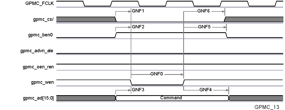
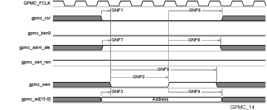
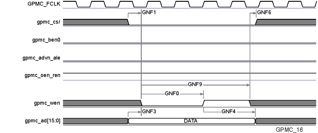
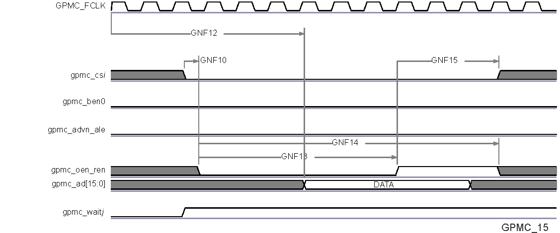
Table 5-53 and Table 5-54 assume testing over the recommended operating conditions and electrical characteristic conditions below (see Figure 5-35, Figure 5-36, Figure 5-37 and Figure 5-38).
Table 5-53 GPMC/NAND Flash Interface Timing Requirements
| NO. | PARAMETER | DESCRIPTION | MIN | MAX | UNIT |
|---|---|---|---|---|---|
| GNF12 | tacc(DAT) | Data maximum access time (GPMC_FCLK Cycles) | J (1) | cycles | |
| - | tsu(DV-OEH) | Setup time, read gpmc_ad[15:0] valid before gpmc_oen_ren high | 1.9 | ns | |
| - | th(OEH-DV) | Hold time, read gpmc_ad[15:0] valid after gpmc_oen_ren high | 1 | ns |
- J = AccessTime × (TimeParaGranularity + 1)
Table 5-54 GPMC/NAND Flash Interface Switching Characteristics
| NO. | PARAMETER | DESCRIPTION | MIN | MAX | UNIT |
|---|---|---|---|---|---|
| - | tr(DO) | Rising time, gpmc_ad[15:0] output data | 0.447 | 4.067 | ns |
| - | tf(DO) | Fallling time, gpmc_ad[15:0] output data | 0.43 | 4.463 | ns |
| GNF0 | tw(nWEV) | Pulse duration, gpmc_wen valid time | A (1) | ns | |
| GNF1 | td(nCSV-nWEV) | Delay time, gpmc_cs[7:0] valid to gpmc_wen valid | B - 2 (2) | B + 4 (2) | ns |
| GNF2 | td(CLEH-nWEV) | Delay time, gpmc_ben[1:0] high to gpmc_wen valid | C - 2 (3) | C + 4 (3) | ns |
| GNF3 | td(nWEV-DV) | Delay time, gpmc_ad[15:0] valid to gpmc_wen valid | D - 2 (4) | D + 4 (4) | ns |
| GNF4 | td(nWEIV-DIV) | Delay time, gpmc_wen invalid to gpmc_ad[15:0] invalid | E - 2 (5) | E + 4 (5) | ns |
| GNF5 | td(nWEIV-CLEIV) | Delay time, gpmc_wen invalid to gpmc_ben[1:0] invalid | F - 2 (6) | F + 4 (6) | ns |
| GNF6 | td(nWEIV-nCSIV) | Delay time, gpmc_wen invalid to gpmc_cs[7:0] invalid | G - 2 (7) | G + 4 (7) | ns |
| GNF7 | td(ALEH-nWEV) | Delay time, gpmc_advn_ale high to gpmc_wen valid | C - 2 (3) | C + 4 (3) | ns |
| GNF8 | td(nWEIV-ALEIV) | Delay time, gpmc_wen invalid to gpmc_advn_ale invalid | F - 2 (6) | F + 4 (6) | ns |
| GNF9 | tc(nWE) | Cycle time, write cycle time | H (8) | ns | |
| GNF10 | td(nCSV-nOEV) | Delay time, gpmc_cs[7:0] valid to gpmc_oen_ren valid | I - 2 (9) | I + 4 (9) | ns |
| GNF13 | tw(nOEV) | Pulse duration, gpmc_oen_ren valid time | K (10) | ns | |
| GNF14 | tc(nOE) | Cycle time, read cycle time | L (11) | ns | |
| GNF15 | td(nOEIV-nCSIV) | Delay time, gpmc_oen_ren invalid to gpmc_cs[7:0] invalid | M - 2 (12) | M + 4 (12) | ns |
- A = (WEOffTime – WEOnTime) × (TimeParaGranularity + 1) × GPMC_FCLK
- B = ((WEOnTime – CSOnTime) × (TimeParaGranularity + 1) + 0.5 × (WEExtraDelay – CSExtraDelay)) × GPMC_FCLK
- C = ((WEOnTime – ADVOnTime) × (TimeParaGranularity + 1) + 0.5 × (WEExtraDelay – ADVExtraDelay)) × GPMC_FCLK
- D = (WEOnTime × (TimeParaGranularity + 1) + 0.5 × WEExtraDelay ) × GPMC_FCLK
- E = (WrCycleTime – WEOffTime × (TimeParaGranularity + 1) – 0.5 × WEExtraDelay ) × GPMC_FCLK
- F = (ADVWrOffTime – WEOffTime × (TimeParaGranularity + 1) + 0.5 × (ADVExtraDelay – WEExtraDelay ) × GPMC_FCLK
- G = (CSWrOffTime – WEOffTime × (TimeParaGranularity + 1) + 0.5 × (CSExtraDelay – WEExtraDelay ) × GPMC_FCLK
- H = WrCycleTime × (1 + TimeParaGranularity) × GPMC_FCLK
- I = ((OEOffTime + (n – 1) × PageBurstAccessTime – CSOnTime) × (TimeParaGranularity + 1) + 0.5 × (OEExtraDelay – CSExtraDelay)) × GPMC_FCLK
- K = (OEOffTime – OEOnTime) × (1 + TimeParaGranularity) × GPMC_FCLK
- L = RdCycleTime × (1 + TimeParaGranularity) × GPMC_FCLK
- M = (CSRdOffTime – OEOffTime × (TimeParaGranularity + 1) + 0.5 × (CSExtraDelay – OEExtraDelay ) × GPMC_FCLK
 Figure 5-35 GPMC / NAND Flash - Command Latch Cycle Timing(1)
 - In gpmc_csi, i = 0 to 7.
 Figure 5-36 GPMC / NAND Flash - Address Latch Cycle Timing(1)
 - In gpmc_csi, i = 0 to 7.
- GNF12 parameter illustrates amount of time required to internally sample input Data. It is expressed in number of GPMC functional clock cycles. From start of read cycle and after GNF12 functional clock cycles, input data will be internally sampled by active functional clock edge. GNF12 value must be stored inside AccessTime register bits field.
- GPMC_FCLK is an internal clock (GPMC functional clock) not provided externally.
- In gpmc_csi, i = 0 to 7. In gpmc_waitj, j = 0 to 1.
 Figure 5-38 GPMC / NAND Flash - Data Write Cycle Timing(1)
 - In gpmc_csi, i = 0 to 7.
NOTE
To configure the desired virtual mode the user must set MODESELECT bit and DELAYMODE bitfield for each corresponding pad control register.
The pad control registers are presented in Table 4-32 and described in Device TRM, Control Module Chapter.
Virtual IO Timings Modes must be used to ensure some IO timings for GPMC. See Table 5-29Modes Summary for a list of IO timings requiring the use of Virtual IO Timings Modes. See Table 5-55Virtual Functions Mapping for GPMC for a definition of the Virtual modes.
Table 5-55 presents the values for DELAYMODE bitfield.
Table 5-55 Virtual Functions Mapping for GPMC
| BALL | BALL NAME | Delay Mode Value | MUXMODE | |||||||
|---|---|---|---|---|---|---|---|---|---|---|
| GPMC_VIRTUAL1 | 0 | 1 | 2 | 3 | 5 | 6 | 14(1) | 14(1) | ||
| H5 | gpmc_advn_ale | 15 | gpmc_advn_ale | gpmc_cs6 | gpmc_wait1 | gpmc_a2 | gpmc_a23 | |||
| B4 | gpmc_ad15 | 13 | gpmc_ad15 | |||||||
| B1 | gpmc_ad6 | 13 | gpmc_ad6 | |||||||
| E1 | gpmc_ad2 | 13 | gpmc_ad2 | |||||||
| E10 | vin2a_d9 | 9 | gpmc_a25 | |||||||
| G6 | gpmc_wen | 15 | gpmc_wen | |||||||
| A3 | gpmc_ad14 | 13 | gpmc_ad14 | |||||||
| H3 | gpmc_a13 | 15 | gpmc_a13 | |||||||
| K4 | gpmc_a8 | 14 | gpmc_a8 | |||||||
| H4 | gpmc_a14 | 15 | gpmc_a14 | |||||||
| D1 | gpmc_ad4 | 13 | gpmc_ad4 | |||||||
| A5 | gpmc_a26 | 15 | gpmc_a26 | gpmc_a20 | ||||||
| F1 | gpmc_ad0 | 13 | gpmc_ad0 | |||||||
| F6 | gpmc_wait0 | 15 | gpmc_wait0 | |||||||
| C10 | vin2a_d11 | 9 | gpmc_a23 | |||||||
| E2 | gpmc_ad1 | 13 | gpmc_ad1 | |||||||
| C4 | gpmc_ad13 | 13 | gpmc_ad13 | |||||||
| L2 | gpmc_a2 | 14 | gpmc_a2 | |||||||
| D2 | gpmc_ad5 | 13 | gpmc_ad5 | |||||||
| B10 | vin2a_d8 | 9 | gpmc_a26 | |||||||
| F3 | gpmc_cs0 | 15 | gpmc_cs0 | |||||||
| E8 | vin2a_hsync0 | 9 | gpmc_a27 | |||||||
| K3 | gpmc_a4 | 14 | gpmc_a4 | |||||||
| H2 | gpmc_ben0 | 15 | gpmc_ben0 | gpmc_cs4 | ||||||
| J1 | gpmc_a6 | 14 | gpmc_a6 | |||||||
| K6 | gpmc_a15 | 15 | gpmc_a15 | |||||||
| B3 | gpmc_ad11 | 13 | gpmc_ad11 | |||||||
| K5 | gpmc_a16 | 15 | gpmc_a16 | |||||||
| M2 | gpmc_a1 | 14 | gpmc_a1 | |||||||
| D7 | gpmc_a24 | 15 | gpmc_a24 | gpmc_a18 | ||||||
| B5 | gpmc_a23 | 15 | gpmc_a23 | gpmc_a17 | ||||||
| C2 | gpmc_ad8 | 13 | gpmc_ad8 | |||||||
| A2 | gpmc_ad10 | 13 | gpmc_ad10 | |||||||
| C3 | gpmc_ad12 | 13 | gpmc_ad12 | |||||||
| E7 | gpmc_a20 | 15 | gpmc_a20 | gpmc_a14 | ||||||
| D10 | vin2a_d10 | 9 | gpmc_a24 | |||||||
| G3 | gpmc_cs3 | 14 | gpmc_cs3 | gpmc_a1 | ||||||
| G5 | gpmc_oen_ren | 15 | gpmc_oen_ren | |||||||
| H1 | gpmc_a9 | 14 | gpmc_a9 | |||||||
| A6 | gpmc_cs1 | 15 | gpmc_cs1 | gpmc_a22 | ||||||
| C1 | gpmc_ad3 | 13 | gpmc_ad3 | |||||||
| B2 | gpmc_ad7 | 13 | gpmc_ad7 | |||||||
| K1 | gpmc_a7 | 14 | gpmc_a7 | |||||||
| L1 | gpmc_a3 | 14 | gpmc_a3 | |||||||
| H6 | gpmc_ben1 | 15 | gpmc_ben1 | gpmc_cs5 | gpmc_a3 | |||||
| L4 | gpmc_clk | 15 | gpmc_clk | gpmc_cs7 | gpmc_wait1 | |||||
| C5 | gpmc_a22 | 15 | gpmc_a22 | gpmc_a16 | ||||||
| G4 | gpmc_cs2 | 15 | gpmc_cs2 | |||||||
| C7 | vin2a_fld0 | 11 | gpmc_a27 | gpmc_a18 | ||||||
| J2 | gpmc_a10 | 14 | gpmc_a10 | |||||||
| G1 | gpmc_a12 | 15 | gpmc_a12 | gpmc_a0 | ||||||
| G2 | gpmc_a17 | 15 | gpmc_a17 | |||||||
| K2 | gpmc_a5 | 14 | gpmc_a5 | |||||||
| D6 | gpmc_a21 | 15 | gpmc_a21 | gpmc_a15 | ||||||
| B6 | gpmc_a27 | 15 | gpmc_a27 | gpmc_a21 | ||||||
| D3 | gpmc_ad9 | 13 | gpmc_ad9 | |||||||
| A4 | gpmc_a19 | 15 | gpmc_a19 | gpmc_a13 | ||||||
| C6 | gpmc_a25 | 15 | gpmc_a25 | gpmc_a19 | ||||||
| M1 | gpmc_a0 | 14 | gpmc_a0 | |||||||
| D8 | vin2a_clk0 | 11 | gpmc_a27 | gpmc_a17 | ||||||
| F2 | gpmc_a18 | 15 | gpmc_a18 | |||||||
| L3 | gpmc_a11 | 14 | gpmc_a11 | |||||||
- Some signals listed are virtual functions that present alternate multiplexing options. These virtual functions are controlled via CTRL_CORE_ALT_SELECT_MUX or CTRL_CORE_VIP_MUX_SELECT registers. For more information on how to use these options, please refer to Device TRM, Chapter Control Module, Section Pad Configuration Registers.
