ZHCSII1F June 2016 – May 2019 DRA710 , DRA712 , DRA714 , DRA716 , DRA718
PRODUCTION DATA.
- 1器件概述
- 2修订历史记录
- 3Device Comparison
-
4Terminal Configuration and Functions
- 4.1 Pin Diagram
- 4.2 Pin Attributes
- 4.3
Signal Descriptions
- 4.3.1 VIP
- 4.3.2 DSS
- 4.3.3 HDMI
- 4.3.4 CSI2
- 4.3.5 EMIF
- 4.3.6 GPMC
- 4.3.7 Timers
- 4.3.8 I2C
- 4.3.9 HDQ1W
- 4.3.10 UART
- 4.3.11 McSPI
- 4.3.12 QSPI
- 4.3.13 McASP
- 4.3.14 USB
- 4.3.15 PCIe
- 4.3.16 DCAN
- 4.3.17 GMAC_SW
- 4.3.18 MLB
- 4.3.19 eMMC/SD/SDIO
- 4.3.20 GPIO
- 4.3.21 KBD
- 4.3.22 PWM
- 4.3.23 PRU-ICSS
- 4.3.24 ATL
- 4.3.25 Emulation and Debug Subsystem
- 4.3.26 System and Miscellaneous
- 4.3.27 Power Supplies
- 4.4 Pin Multiplexing
- 4.5 Connections for Unused Pins
-
5Specifications
- 5.1 Absolute Maximum Ratings
- 5.2 ESD Ratings
- 5.3 Power on Hours (POH) Limits
- 5.4 Recommended Operating Conditions
- 5.5 Operating Performance Points
- 5.6 Power Consumption Summary
- 5.7
Electrical Characteristics
- Table 5-6 LVCMOS DDR DC Electrical Characteristics
- Table 5-7 Dual Voltage LVCMOS I2C DC Electrical Characteristics
- Table 5-8 IQ1833 Buffers DC Electrical Characteristics
- Table 5-9 IHHV1833 Buffers DC Electrical Characteristics
- Table 5-10 LVCMOS CSI2 DC Electrical Characteristics
- Table 5-11 BMLB18 Buffers DC Electrical Characteristics
- Table 5-12 Dual Voltage SDIO1833 DC Electrical Characteristics
- Table 5-13 Dual Voltage LVCMOS DC Electrical Characteristics
- 5.7.1 USBPHY DC Electrical Characteristics
- 5.7.2 HDMIPHY DC Electrical Characteristics
- 5.7.3 PCIEPHY DC Electrical Characteristics
- 5.8 VPP Specifications for One-Time Programmable (OTP) eFuses
- 5.9 Thermal Resistance Characteristics for CBD Package
- 5.10
Timing Requirements and Switching Characteristics
- 5.10.1 Timing Parameters and Information
- 5.10.2 Interface Clock Specifications
- 5.10.3 Power Supply Sequences
- 5.10.4 Clock Specifications
- 5.10.5 Recommended Clock and Control Signal Transition Behavior
- 5.10.6
Peripherals
- 5.10.6.1 Timing Test Conditions
- 5.10.6.2 Virtual and Manual I/O Timing Modes
- 5.10.6.3 VIP
- 5.10.6.4 DSS
- 5.10.6.5 HDMI
- 5.10.6.6 CSI2
- 5.10.6.7 EMIF
- 5.10.6.8 GPMC
- 5.10.6.9 Timers
- 5.10.6.10 I2C
- 5.10.6.11 HDQ1W
- 5.10.6.12 UART
- 5.10.6.13 McSPI
- 5.10.6.14 QSPI
- 5.10.6.15 McASP
- 5.10.6.16 USB
- 5.10.6.17 PCIe
- 5.10.6.18 DCAN
- 5.10.6.19
GMAC_SW
- 5.10.6.19.1
GMAC MII Timings
- Table 5-93 Timing Requirements for miin_rxclk - MII Operation
- Table 5-94 Timing Requirements for miin_txclk - MII Operation
- Table 5-95 Timing Requirements for GMAC MIIn Receive 10/100 Mbit/s
- Table 5-96 Switching Characteristics Over Recommended Operating Conditions for GMAC MIIn Transmit 10/100 Mbits/s
- 5.10.6.19.2 GMAC MDIO Interface Timings
- 5.10.6.19.3
GMAC RMII Timings
- Table 5-101 Timing Requirements for GMAC REF_CLK - RMII Operation
- Table 5-102 Timing Requirements for GMAC RMIIn Receive
- Table 5-103 Switching Characteristics Over Recommended Operating Conditions for GMAC REF_CLK - RMII Operation
- Table 5-104 Switching Characteristics Over Recommended Operating Conditions for GMAC RMIIn Transmit 10/100 Mbits/s
- 5.10.6.19.4
GMAC RGMII Timings
- Table 5-108 Timing Requirements for rgmiin_rxc - RGMIIn Operation
- Table 5-109 Timing Requirements for GMAC RGMIIn Input Receive for 10/100/1000 Mbps
- Table 5-110 Switching Characteristics Over Recommended Operating Conditions for rgmiin_txctl - RGMIIn Operation for 10/100/1000 Mbit/s
- Table 5-111 Switching Characteristics for GMAC RGMIIn Output Transmit for 10/100/1000 Mbps
- 5.10.6.19.1
GMAC MII Timings
- 5.10.6.20 MLB
- 5.10.6.21
eMMC/SD/SDIO
- 5.10.6.21.1
MMC1—SD Card Interface
- 5.10.6.21.1.1 Default speed, 4-bit data, SDR, half-cycle
- 5.10.6.21.1.2 High speed, 4-bit data, SDR, half-cycle
- 5.10.6.21.1.3 SDR12, 4-bit data, half-cycle
- 5.10.6.21.1.4 SDR25, 4-bit data, half-cycle
- 5.10.6.21.1.5 UHS-I SDR50, 4-bit data, half-cycle
- 5.10.6.21.1.6 UHS-I SDR104, 4-bit data, half-cycle
- 5.10.6.21.1.7 UHS-I DDR50, 4-bit data
- 5.10.6.21.2 MMC2 — eMMC
- 5.10.6.21.3 MMC3 and MMC4—SDIO/SD
- 5.10.6.21.1
MMC1—SD Card Interface
- 5.10.6.22 GPIO
- 5.10.6.23
PRU-ICSS
- 5.10.6.23.1 Programmable Real-Time Unit (PRU-ICSS PRU)
- 5.10.6.23.2
PRU-ICSS EtherCAT (PRU-ICSS ECAT)
- 5.10.6.23.2.1
PRU-ICSS ECAT Electrical Data and Timing
- Table 5-172 PRU-ICSS ECAT Timing Requirements – Input Validated With LATCH_IN
- Table 5-173 PRU-ICSS ECAT Timing Requirements – Input Validated With SYNCx
- Table 5-174 PRU-ICSS ECAT Timing Requirements – Input Validated With Start of Frame (SOF)
- Table 5-175 PRU-ICSS ECAT Timing Requirements - LATCHx_IN
- Table 5-176 PRU-ICSS ECAT Switching Requirements - Digital IOs
- 5.10.6.23.2.1
PRU-ICSS ECAT Electrical Data and Timing
- 5.10.6.23.3 PRU-ICSS MII_RT and Switch
- 5.10.6.23.4 PRU-ICSS Universal Asynchronous Receiver Transmitter (PRU-ICSS UART)
- 5.10.6.23.5 PRU-ICSS IOSETs
- 5.10.6.23.6 PRU-ICSS Manual Functional Mapping
- 5.10.6.24 System and Miscellaneous interfaces
- 5.10.7
Emulation and Debug Subsystem
- 5.10.7.1
IEEE 1149.1 Standard-Test-Access Port (JTAG)
- 5.10.7.1.1
JTAG Electrical Data/Timing
- Table 5-202 Timing Requirements for IEEE 1149.1 JTAG
- Table 5-203 Switching Characteristics Over Recommended Operating Conditions for IEEE 1149.1 JTAG
- Table 5-204 Timing Requirements for IEEE 1149.1 JTAG With RTCK
- Table 5-205 Switching Characteristics Over Recommended Operating Conditions for IEEE 1149.1 JTAG With RTCK
- 5.10.7.1.1
JTAG Electrical Data/Timing
- 5.10.7.2 Trace Port Interface Unit (TPIU)
- 5.10.7.1
IEEE 1149.1 Standard-Test-Access Port (JTAG)
-
6Detailed Description
- 6.1 Description
- 6.2 Functional Block Diagram
- 6.3 MPU
- 6.4 DSP Subsystem
- 6.5 IVA
- 6.6 IPU
- 6.7 GPU
- 6.8 BB2D
- 6.9 PRU-ICSS
- 6.10 Memory Subsystem
- 6.11 Interprocessor Communication
- 6.12 Interrupt Controller
- 6.13 EDMA
- 6.14 Peripherals
- 6.15 On-chip Debug
-
7Applications, Implementation, and Layout
- 7.1 Introduction
- 7.2 Power Optimizations
- 7.3 Core Power Domains
- 7.4 Single-Ended Interfaces
- 7.5
Differential Interfaces
- 7.5.1 General Routing Guidelines
- 7.5.2
USB 2.0 Board Design and Layout Guidelines
- 7.5.2.1 Background
- 7.5.2.2
USB PHY Layout Guide
- 7.5.2.2.1 General Routing and Placement
- 7.5.2.2.2
Specific Guidelines for USB PHY Layout
- 7.5.2.2.2.1 Analog, PLL, and Digital Power Supply Filtering
- 7.5.2.2.2.2 Analog, Digital, and PLL Partitioning
- 7.5.2.2.2.3 Board Stackup
- 7.5.2.2.2.4 Cable Connector Socket
- 7.5.2.2.2.5 Clock Routings
- 7.5.2.2.2.6 Crystals/Oscillator
- 7.5.2.2.2.7 DP/DM Trace
- 7.5.2.2.2.8 DP/DM Vias
- 7.5.2.2.2.9 Image Planes
- 7.5.2.2.2.10 Power Regulators
- 7.5.2.3 References
- 7.5.3 USB 3.0 Board Design and Layout Guidelines
- 7.5.4 HDMI Board Design and Layout Guidelines
- 7.5.5 PCIe Board Design and Layout Guidelines
- 7.5.6 CSI2 Board Design and Routing Guidelines
- 7.6 Clock Routing Guidelines
- 7.7
DDR3 Board Design and Layout Guidelines
- 7.7.1 DDR3 General Board Layout Guidelines
- 7.7.2
DDR3 Board Design and Layout Guidelines
- 7.7.2.1 Board Designs
- 7.7.2.2 DDR3 EMIF
- 7.7.2.3 DDR3 Device Combinations
- 7.7.2.4 DDR3 Interface Schematic
- 7.7.2.5 Compatible JEDEC DDR3 Devices
- 7.7.2.6 PCB Stackup
- 7.7.2.7 Placement
- 7.7.2.8 DDR3 Keepout Region
- 7.7.2.9 Bulk Bypass Capacitors
- 7.7.2.10 High-Speed Bypass Capacitors
- 7.7.2.11 Net Classes
- 7.7.2.12 DDR3 Signal Termination
- 7.7.2.13 VREF_DDR Routing
- 7.7.2.14 VTT
- 7.7.2.15 CK and ADDR_CTRL Topologies and Routing Definition
- 7.7.2.16 Data Topologies and Routing Definition
- 7.7.2.17 Routing Specification
- 8Device and Documentation Support
- 9Mechanical, Packaging, and Orderable Information
7.3.8.2 vdd Example Analysis
Maximum acceptable PCB resistance (Reff) between the PMIC and Processor input power balls should not exceed 10mΩ.
Maximum decoupling capacitance loop inductance (LL) between Processor input power balls and decoupling capacitances should not exceed 2.0nH (ESL NOT included)
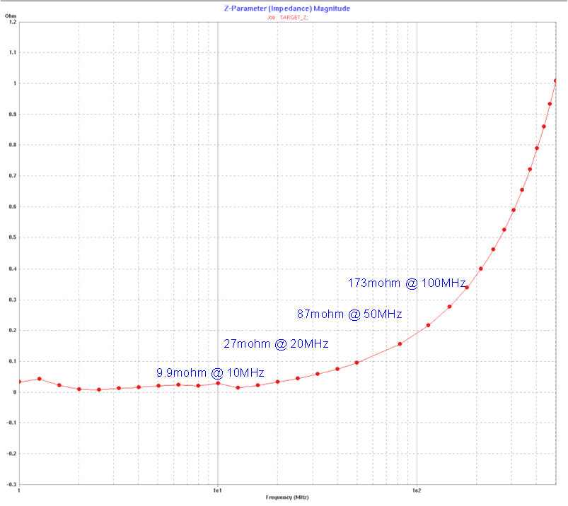
Impedance target for key frequency of interest between Processor input power balls and PMIC’s SMPS output power balls should not exceed 57mΩ at 20MHz.
Table 7-7 Example PCB vdd PI Analysis Summary
| Parameter | Recommendation | Example PCB |
|---|---|---|
| OPP | OPP_NOM | |
| Clocking Rate | 266 MHz | |
| Voltage Level | 1 V | 1 V |
| Max Current Draw | 1 A | 1 A |
| Max Effective Resistance: Power Inductor Segment Total Reff | 10mΩ | 9.7 mΩ |
| Max Loop Inductance | 2.0nH | 0.97 –1.75nH |
| Impedance Target | 57mΩ F<20Mhz | 57mΩ F<20Mhz |
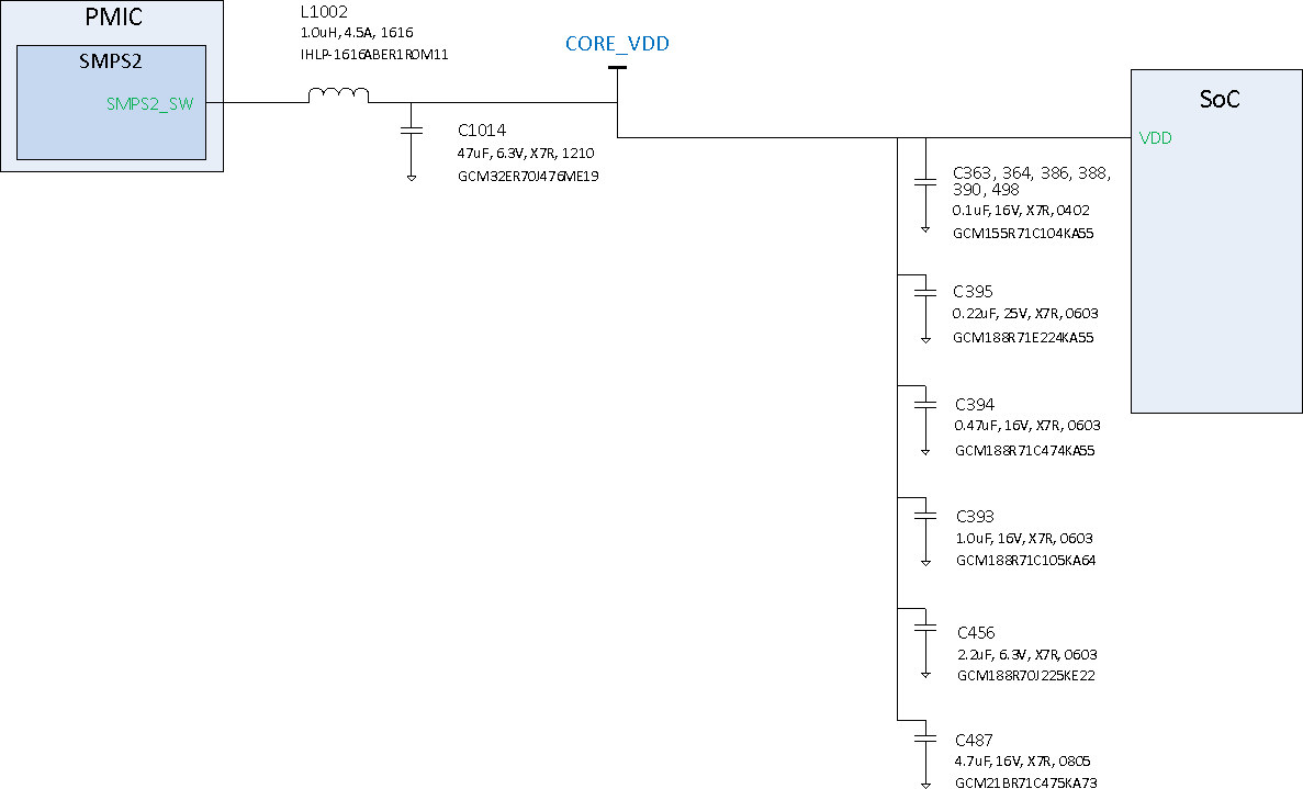
Figure 7-15 show a PCB layout example and the resulting PI analysis results.
 Figure 7-15 vdd Simplified SCH Diagram
 NOTE
PCB Etch Resistance Breakdown, PDN Effective Resistance, and vdd routings are UNDER DEVELOPMENT!
IR Drop: vdd (PCB Rev Oct25, CAD sPSI v13.1.1)
- Source Conditions: 1V @ 1A
- Power Plane/Trace Effective Resistances
- From PMIC SMPS to SoC load = 9.7mohm
- From Power Inductor to SoC load = 6mohm
- "Open-Loop" Voltage/IR Drop for 1A = 6mV
![DRA710 DRA712 DRA714 DRA716 DRA718 vdd Voltage/IR Drop [All Layers] DRA710 DRA712 DRA714 DRA716 DRA718 SPRS906_PCB_CORE_06.gif](/ods/images/ZHCSII1F/SPRS906_PCB_CORE_06.gif) Figure 7-16 vdd Voltage/IR Drop [All Layers]
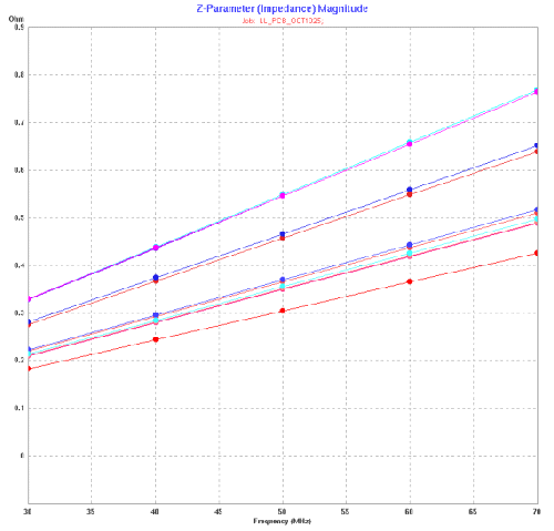
Figure 7-16 vdd Voltage/IR Drop [All Layers] Dynamic analysis of this PCB design for the CORE power domain determined the vdd decoupling capacitor loop inductance and impedance vs frequency analysis shown below. As you can see, the loop inductance values ranged from 0.97 –1.75nH and were less than maximum 2.0nH recommended.
NOTE
Comparing loop inductances for capacitors at different distances from the SoC’s input power balls shows an 18% reduction for caps placed closer. This was derived by averaging the inductances for the 3 caps with distances over 800mils (Avg LL = 1.33nH) vs the 3 caps with distances less than 600mils (Avg LL = 1.096nH).
Table 7-8 Rail - vdd
| Cap Ref Des | Model Port # | Loop Inductacne [nH] | Footprint Types | PCB Side | Distance to Ball-Field [mils] | Value [μF] | Size |
|---|---|---|---|---|---|---|---|
| C487 | 10 | 0.97 | 4vWSE | Top | 521 | 4.7 | 0805 |
| C393 | 6 | 1.11 | 4vWSE | Bottom | 358 | 1.0 | 0603 |
| C394 | 7 | 1.12 | 4vWSE | Bottom | 357 | 0.47 | 0603 |
| C456 | 9 | 1.13 | 4vWSE | Bottom | 403 | 2.2 | 0603 |
| C386 | 3 | 1.16 | 2vWSE | Bottom | 40 | 0.1 | 0402 |
| C395 | 8 | 1.18 | 4vWSE | Bottom | 460 | 0.22 | 0603 |
| C363 | 1 | 1.46 | 2vWSE | Bottom | 40 | 0.1 | 0402 |
| C390 | 5 | 1.48 | 2vWSE | Bottom | 40 | 0.1 | 0402 |
| C364 | 2 | 1.74 | 2vWSE | Bottom | 40 | 0.1 | 0402 |
| C498 | 11 | 1.74 | 2vWSE | Bottom | 40 | 0.1 | 0402 |
| C388 | 4 | 1.75 | 2vWSE | Bottom | 40 | 0.1 | 0402 |
Loop Inductance range: 0.97 –1.75nH
 Figure 7-17 vdd Decoupling Cap Loop Inductances
 Figure 7-18 shows vdd Impedance vs Frequency characteristics.
 Figure 7-18 vdd Impedance vs Frequency