ZHCSII1F June 2016 – May 2019 DRA710 , DRA712 , DRA714 , DRA716 , DRA718
PRODUCTION DATA.
- 1器件概述
- 2修订历史记录
- 3Device Comparison
-
4Terminal Configuration and Functions
- 4.1 Pin Diagram
- 4.2 Pin Attributes
- 4.3
Signal Descriptions
- 4.3.1 VIP
- 4.3.2 DSS
- 4.3.3 HDMI
- 4.3.4 CSI2
- 4.3.5 EMIF
- 4.3.6 GPMC
- 4.3.7 Timers
- 4.3.8 I2C
- 4.3.9 HDQ1W
- 4.3.10 UART
- 4.3.11 McSPI
- 4.3.12 QSPI
- 4.3.13 McASP
- 4.3.14 USB
- 4.3.15 PCIe
- 4.3.16 DCAN
- 4.3.17 GMAC_SW
- 4.3.18 MLB
- 4.3.19 eMMC/SD/SDIO
- 4.3.20 GPIO
- 4.3.21 KBD
- 4.3.22 PWM
- 4.3.23 PRU-ICSS
- 4.3.24 ATL
- 4.3.25 Emulation and Debug Subsystem
- 4.3.26 System and Miscellaneous
- 4.3.27 Power Supplies
- 4.4 Pin Multiplexing
- 4.5 Connections for Unused Pins
-
5Specifications
- 5.1 Absolute Maximum Ratings
- 5.2 ESD Ratings
- 5.3 Power on Hours (POH) Limits
- 5.4 Recommended Operating Conditions
- 5.5 Operating Performance Points
- 5.6 Power Consumption Summary
- 5.7
Electrical Characteristics
- Table 5-6 LVCMOS DDR DC Electrical Characteristics
- Table 5-7 Dual Voltage LVCMOS I2C DC Electrical Characteristics
- Table 5-8 IQ1833 Buffers DC Electrical Characteristics
- Table 5-9 IHHV1833 Buffers DC Electrical Characteristics
- Table 5-10 LVCMOS CSI2 DC Electrical Characteristics
- Table 5-11 BMLB18 Buffers DC Electrical Characteristics
- Table 5-12 Dual Voltage SDIO1833 DC Electrical Characteristics
- Table 5-13 Dual Voltage LVCMOS DC Electrical Characteristics
- 5.7.1 USBPHY DC Electrical Characteristics
- 5.7.2 HDMIPHY DC Electrical Characteristics
- 5.7.3 PCIEPHY DC Electrical Characteristics
- 5.8 VPP Specifications for One-Time Programmable (OTP) eFuses
- 5.9 Thermal Resistance Characteristics for CBD Package
- 5.10
Timing Requirements and Switching Characteristics
- 5.10.1 Timing Parameters and Information
- 5.10.2 Interface Clock Specifications
- 5.10.3 Power Supply Sequences
- 5.10.4 Clock Specifications
- 5.10.5 Recommended Clock and Control Signal Transition Behavior
- 5.10.6
Peripherals
- 5.10.6.1 Timing Test Conditions
- 5.10.6.2 Virtual and Manual I/O Timing Modes
- 5.10.6.3 VIP
- 5.10.6.4 DSS
- 5.10.6.5 HDMI
- 5.10.6.6 CSI2
- 5.10.6.7 EMIF
- 5.10.6.8 GPMC
- 5.10.6.9 Timers
- 5.10.6.10 I2C
- 5.10.6.11 HDQ1W
- 5.10.6.12 UART
- 5.10.6.13 McSPI
- 5.10.6.14 QSPI
- 5.10.6.15 McASP
- 5.10.6.16 USB
- 5.10.6.17 PCIe
- 5.10.6.18 DCAN
- 5.10.6.19
GMAC_SW
- 5.10.6.19.1
GMAC MII Timings
- Table 5-93 Timing Requirements for miin_rxclk - MII Operation
- Table 5-94 Timing Requirements for miin_txclk - MII Operation
- Table 5-95 Timing Requirements for GMAC MIIn Receive 10/100 Mbit/s
- Table 5-96 Switching Characteristics Over Recommended Operating Conditions for GMAC MIIn Transmit 10/100 Mbits/s
- 5.10.6.19.2 GMAC MDIO Interface Timings
- 5.10.6.19.3
GMAC RMII Timings
- Table 5-101 Timing Requirements for GMAC REF_CLK - RMII Operation
- Table 5-102 Timing Requirements for GMAC RMIIn Receive
- Table 5-103 Switching Characteristics Over Recommended Operating Conditions for GMAC REF_CLK - RMII Operation
- Table 5-104 Switching Characteristics Over Recommended Operating Conditions for GMAC RMIIn Transmit 10/100 Mbits/s
- 5.10.6.19.4
GMAC RGMII Timings
- Table 5-108 Timing Requirements for rgmiin_rxc - RGMIIn Operation
- Table 5-109 Timing Requirements for GMAC RGMIIn Input Receive for 10/100/1000 Mbps
- Table 5-110 Switching Characteristics Over Recommended Operating Conditions for rgmiin_txctl - RGMIIn Operation for 10/100/1000 Mbit/s
- Table 5-111 Switching Characteristics for GMAC RGMIIn Output Transmit for 10/100/1000 Mbps
- 5.10.6.19.1
GMAC MII Timings
- 5.10.6.20 MLB
- 5.10.6.21
eMMC/SD/SDIO
- 5.10.6.21.1
MMC1—SD Card Interface
- 5.10.6.21.1.1 Default speed, 4-bit data, SDR, half-cycle
- 5.10.6.21.1.2 High speed, 4-bit data, SDR, half-cycle
- 5.10.6.21.1.3 SDR12, 4-bit data, half-cycle
- 5.10.6.21.1.4 SDR25, 4-bit data, half-cycle
- 5.10.6.21.1.5 UHS-I SDR50, 4-bit data, half-cycle
- 5.10.6.21.1.6 UHS-I SDR104, 4-bit data, half-cycle
- 5.10.6.21.1.7 UHS-I DDR50, 4-bit data
- 5.10.6.21.2 MMC2 — eMMC
- 5.10.6.21.3 MMC3 and MMC4—SDIO/SD
- 5.10.6.21.1
MMC1—SD Card Interface
- 5.10.6.22 GPIO
- 5.10.6.23
PRU-ICSS
- 5.10.6.23.1 Programmable Real-Time Unit (PRU-ICSS PRU)
- 5.10.6.23.2
PRU-ICSS EtherCAT (PRU-ICSS ECAT)
- 5.10.6.23.2.1
PRU-ICSS ECAT Electrical Data and Timing
- Table 5-172 PRU-ICSS ECAT Timing Requirements – Input Validated With LATCH_IN
- Table 5-173 PRU-ICSS ECAT Timing Requirements – Input Validated With SYNCx
- Table 5-174 PRU-ICSS ECAT Timing Requirements – Input Validated With Start of Frame (SOF)
- Table 5-175 PRU-ICSS ECAT Timing Requirements - LATCHx_IN
- Table 5-176 PRU-ICSS ECAT Switching Requirements - Digital IOs
- 5.10.6.23.2.1
PRU-ICSS ECAT Electrical Data and Timing
- 5.10.6.23.3 PRU-ICSS MII_RT and Switch
- 5.10.6.23.4 PRU-ICSS Universal Asynchronous Receiver Transmitter (PRU-ICSS UART)
- 5.10.6.23.5 PRU-ICSS IOSETs
- 5.10.6.23.6 PRU-ICSS Manual Functional Mapping
- 5.10.6.24 System and Miscellaneous interfaces
- 5.10.7
Emulation and Debug Subsystem
- 5.10.7.1
IEEE 1149.1 Standard-Test-Access Port (JTAG)
- 5.10.7.1.1
JTAG Electrical Data/Timing
- Table 5-202 Timing Requirements for IEEE 1149.1 JTAG
- Table 5-203 Switching Characteristics Over Recommended Operating Conditions for IEEE 1149.1 JTAG
- Table 5-204 Timing Requirements for IEEE 1149.1 JTAG With RTCK
- Table 5-205 Switching Characteristics Over Recommended Operating Conditions for IEEE 1149.1 JTAG With RTCK
- 5.10.7.1.1
JTAG Electrical Data/Timing
- 5.10.7.2 Trace Port Interface Unit (TPIU)
- 5.10.7.1
IEEE 1149.1 Standard-Test-Access Port (JTAG)
-
6Detailed Description
- 6.1 Description
- 6.2 Functional Block Diagram
- 6.3 MPU
- 6.4 DSP Subsystem
- 6.5 IVA
- 6.6 IPU
- 6.7 GPU
- 6.8 BB2D
- 6.9 PRU-ICSS
- 6.10 Memory Subsystem
- 6.11 Interprocessor Communication
- 6.12 Interrupt Controller
- 6.13 EDMA
- 6.14 Peripherals
- 6.15 On-chip Debug
-
7Applications, Implementation, and Layout
- 7.1 Introduction
- 7.2 Power Optimizations
- 7.3 Core Power Domains
- 7.4 Single-Ended Interfaces
- 7.5
Differential Interfaces
- 7.5.1 General Routing Guidelines
- 7.5.2
USB 2.0 Board Design and Layout Guidelines
- 7.5.2.1 Background
- 7.5.2.2
USB PHY Layout Guide
- 7.5.2.2.1 General Routing and Placement
- 7.5.2.2.2
Specific Guidelines for USB PHY Layout
- 7.5.2.2.2.1 Analog, PLL, and Digital Power Supply Filtering
- 7.5.2.2.2.2 Analog, Digital, and PLL Partitioning
- 7.5.2.2.2.3 Board Stackup
- 7.5.2.2.2.4 Cable Connector Socket
- 7.5.2.2.2.5 Clock Routings
- 7.5.2.2.2.6 Crystals/Oscillator
- 7.5.2.2.2.7 DP/DM Trace
- 7.5.2.2.2.8 DP/DM Vias
- 7.5.2.2.2.9 Image Planes
- 7.5.2.2.2.10 Power Regulators
- 7.5.2.3 References
- 7.5.3 USB 3.0 Board Design and Layout Guidelines
- 7.5.4 HDMI Board Design and Layout Guidelines
- 7.5.5 PCIe Board Design and Layout Guidelines
- 7.5.6 CSI2 Board Design and Routing Guidelines
- 7.6 Clock Routing Guidelines
- 7.7
DDR3 Board Design and Layout Guidelines
- 7.7.1 DDR3 General Board Layout Guidelines
- 7.7.2
DDR3 Board Design and Layout Guidelines
- 7.7.2.1 Board Designs
- 7.7.2.2 DDR3 EMIF
- 7.7.2.3 DDR3 Device Combinations
- 7.7.2.4 DDR3 Interface Schematic
- 7.7.2.5 Compatible JEDEC DDR3 Devices
- 7.7.2.6 PCB Stackup
- 7.7.2.7 Placement
- 7.7.2.8 DDR3 Keepout Region
- 7.7.2.9 Bulk Bypass Capacitors
- 7.7.2.10 High-Speed Bypass Capacitors
- 7.7.2.11 Net Classes
- 7.7.2.12 DDR3 Signal Termination
- 7.7.2.13 VREF_DDR Routing
- 7.7.2.14 VTT
- 7.7.2.15 CK and ADDR_CTRL Topologies and Routing Definition
- 7.7.2.16 Data Topologies and Routing Definition
- 7.7.2.17 Routing Specification
- 8Device and Documentation Support
- 9Mechanical, Packaging, and Orderable Information
7.7.2.15.2.2 CK and ADDR_CTRL Routing, Two DDR3 Devices
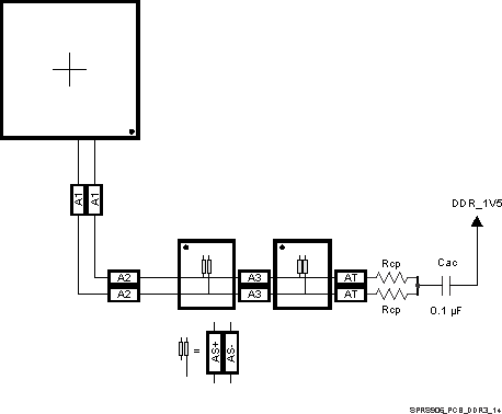
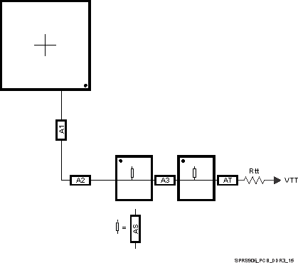
Figure 7-50 shows the CK routing for two DDR3 devices placed on the same side of the PCB. Figure 7-51 shows the corresponding ADDR_CTRL routing.
 Figure 7-50 CK Routing for Two Single-Side DDR3 Devices
  Figure 7-51 ADDR_CTRL Routing for Two Single-Side DDR3 Devices
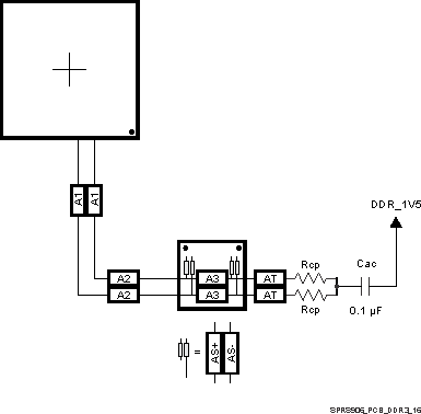
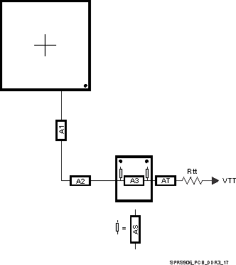
 To save PCB space, the two DDR3 memories may be mounted as a mirrored pair at a cost of increased routing and assembly complexity. Figure 7-52 and Figure 7-53 show the routing for CK and ADDR_CTRL, respectively, for two DDR3 devices mirrored in a single-pair configuration.
 Figure 7-52 CK Routing for Two Mirrored DDR3 Devices
  Figure 7-53 ADDR_CTRL Routing for Two Mirrored DDR3 Devices