ZHCSIC7H March 2016 – November 2019 DRA722 , DRA724 , DRA725 , DRA726
PRODUCTION DATA.
- 1 器件概述
- 2 修订历史记录
- 3 Device Comparison
-
4 Terminal Configuration and Functions
- 4.1 Terminal Assignment
- 4.2 Ball Characteristics
- 4.3 Multiplexing Characteristics
- 4.4
Signal Descriptions
- 4.4.1 Video Input Ports (VIP)
- 4.4.2 Display Subsystem – Video Output Ports
- 4.4.3 Display Subsystem – High-Definition Multimedia Interface (HDMI)
- 4.4.4 Camera Serial Interface 2 CAL bridge (CSI2)
- 4.4.5 External Memory Interface (EMIF)
- 4.4.6 General-Purpose Memory Controller (GPMC)
- 4.4.7 Timers
- 4.4.8 Inter-Integrated Circuit Interface (I2C)
- 4.4.9 HDQ / 1-Wire Interface (HDQ1W)
- 4.4.10 Universal Asynchronous Receiver Transmitter (UART)
- 4.4.11 Multichannel Serial Peripheral Interface (McSPI)
- 4.4.12 Quad Serial Peripheral Interface (QSPI)
- 4.4.13 Multicannel Audio Serial Port (McASP)
- 4.4.14 Universal Serial Bus (USB)
- 4.4.15 SATA
- 4.4.16 Peripheral Component Interconnect Express (PCIe)
- 4.4.17 Controller Area Network Interface (DCAN)
- 4.4.18 Ethernet Interface (GMAC_SW)
- 4.4.19 Media Local Bus (MLB) Interface
- 4.4.20 eMMC/SD/SDIO
- 4.4.21 General-Purpose Interface (GPIO)
- 4.4.22 Keyboard controller (KBD)
- 4.4.23 Pulse Width Modulation (PWM) Interface
- 4.4.24 Audio Tracking Logic (ATL)
- 4.4.25 Test Interfaces
- 4.4.26 System and Miscellaneous
- 4.4.27 Power Supplies
-
5 Specifications
- 5.1 Absolute Maximum Ratings
- 5.2 ESD Ratings
- 5.3 Power-On-Hour (POH) Limits
- 5.4 Recommended Operating Conditions
- 5.5 Operating Performance Points
- 5.6 Power Consumption Summary
- 5.7
Electrical Characteristics
- 5.7.1 LVCMOS DDR DC Electrical Characteristics
- 5.7.2 HDMIPHY DC Electrical Characteristics
- 5.7.3 Dual Voltage LVCMOS I2C DC Electrical Characteristics
- 5.7.4 IQ1833 Buffers DC Electrical Characteristics
- 5.7.5 IHHV1833 Buffers DC Electrical Characteristics
- 5.7.6 LVCMOS OSC Buffers DC Electrical Characteristics
- 5.7.7 LVCMOS CSI2 DC Electrical Characteristics
- 5.7.8 BMLB18 Buffers DC Electrical Characteristics
- 5.7.9 BC1833IHHV Buffers DC Electrical Characteristics
- 5.7.10 USBPHY DC Electrical Characteristics
- 5.7.11 Dual Voltage SDIO1833 DC Electrical Characteristics
- 5.7.12 Dual Voltage LVCMOS DC Electrical Characteristics
- 5.7.13 SATAPHY DC Electrical Characteristics
- 5.7.14 PCIEPHY DC Electrical Characteristics
- 5.8 VPP Specifications for One-Time Programmable (OTP) eFuses
- 5.9 Thermal Characteristics
- 5.10 Power Supply Sequences
- 6 Clock Specifications
-
7 Timing Requirements and Switching Characteristics
- 7.1 Timing Test Conditions
- 7.2 Interface Clock Specifications
- 7.3 Timing Parameters and Information
- 7.4 Recommended Clock and Control Signal Transition Behavior
- 7.5 Virtual and Manual I/O Timing Modes
- 7.6 Video Input Ports (VIP)
- 7.7 Display Subsystem - Video Output Ports
- 7.8 Display Subsystem - High-Definition Multimedia Interface (HDMI)
- 7.9 Camera Serial Interface 2 CAL bridge (CSI2)
- 7.10 External Memory Interface (EMIF)
- 7.11 General-Purpose Memory Controller (GPMC)
- 7.12 Timers
- 7.13 Inter-Integrated Circuit Interface (I2C)
- 7.14 HDQ / 1-Wire Interface (HDQ1W)
- 7.15 Universal Asynchronous Receiver Transmitter (UART)
- 7.16 Multichannel Serial Peripheral Interface (McSPI)
- 7.17 Quad Serial Peripheral Interface (QSPI)
- 7.18 Multichannel Audio Serial Port (McASP)
- 7.19 Universal Serial Bus (USB)
- 7.20 Serial Advanced Technology Attachment (SATA)
- 7.21 Peripheral Component Interconnect Express (PCIe)
- 7.22 Controller Area Network Interface (DCAN)
- 7.23
Ethernet Interface (GMAC_SW)
- 7.23.1
GMAC MII Timings
- Table 7-70 Timing Requirements for miin_rxclk - MII Operation
- Table 7-71 Timing Requirements for miin_txclk - MII Operation
- Table 7-72 Timing Requirements for GMAC MIIn Receive 10/100 Mbit/s
- Table 7-73 Switching Characteristics Over Recommended Operating Conditions for GMAC MIIn Transmit 10/100 Mbits/s
- 7.23.2 GMAC MDIO Interface Timings
- 7.23.3
GMAC RMII Timings
- Table 7-78 Timing Requirements for GMAC REF_CLK - RMII Operation
- Table 7-79 Timing Requirements for GMAC RMIIn Receive
- Table 7-80 Switching Characteristics Over Recommended Operating Conditions for GMAC REF_CLK - RMII Operation
- Table 7-81 Switching Characteristics Over Recommended Operating Conditions for GMAC RMIIn Transmit 10/100 Mbits/s
- 7.23.4
GMAC RGMII Timings
- Table 7-85 Timing Requirements for rgmiin_rxc - RGMIIn Operation
- Table 7-86 Timing Requirements for GMAC RGMIIn Input Receive for 10/100/1000 Mbps
- Table 7-87 Switching Characteristics Over Recommended Operating Conditions for rgmiin_txctl - RGMIIn Operation for 10/100/1000 Mbit/s
- Table 7-88 Switching Characteristics for GMAC RGMIIn Output Transmit for 10/100/1000 Mbps
- 7.23.1
GMAC MII Timings
- 7.24 Media Local Bus (MLB) interface
- 7.25
eMMC/SD/SDIO
- 7.25.1
MMC1-SD Card Interface
- 7.25.1.1 Default speed, 4-bit data, SDR, half-cycle
- 7.25.1.2 High speed, 4-bit data, SDR, half-cycle
- 7.25.1.3 SDR12, 4-bit data, half-cycle
- 7.25.1.4 SDR25, 4-bit data, half-cycle
- 7.25.1.5 UHS-I SDR50, 4-bit data, half-cycle
- 7.25.1.6 UHS-I SDR104, 4-bit data, half-cycle
- 7.25.1.7 UHS-I DDR50, 4-bit data
- 7.25.2 MMC2 - eMMC
- 7.25.3 MMC3 and MMC4-SDIO/SD
- 7.25.1
MMC1-SD Card Interface
- 7.26 General-Purpose Interface (GPIO)
- 7.27 Audio Tracking Logic (ATL)
- 7.28 System and Miscellaneous interfaces
- 7.29
Test Interfaces
- 7.29.1
IEEE 1149.1 Standard-Test-Access Port (JTAG)
- 7.29.1.1
JTAG Electrical Data/Timing
- Table 7-142 Timing Requirements for IEEE 1149.1 JTAG
- Table 7-143 Switching Characteristics Over Recommended Operating Conditions for IEEE 1149.1 JTAG
- Table 7-144 Timing Requirements for IEEE 1149.1 JTAG With RTCK
- Table 7-145 Switching Characteristics Over Recommended Operating Conditions for IEEE 1149.1 JTAG With RTCK
- 7.29.1.1
JTAG Electrical Data/Timing
- 7.29.2 Trace Port Interface Unit (TPIU)
- 7.29.1
IEEE 1149.1 Standard-Test-Access Port (JTAG)
-
8 Applications, Implementation, and Layout
- 8.1 Introduction
- 8.2 Power Optimizations
- 8.3 Core Power Domains
- 8.4 Single-Ended Interfaces
- 8.5
Differential Interfaces
- 8.5.1 General Routing Guidelines
- 8.5.2
USB 2.0 Board Design and Layout Guidelines
- 8.5.2.1 Background
- 8.5.2.2
USB PHY Layout Guide
- 8.5.2.2.1 General Routing and Placement
- 8.5.2.2.2
Specific Guidelines for USB PHY Layout
- 8.5.2.2.2.1 Analog, PLL, and Digital Power Supply Filtering
- 8.5.2.2.2.2 Analog, Digital, and PLL Partitioning
- 8.5.2.2.2.3 Board Stackup
- 8.5.2.2.2.4 Cable Connector Socket
- 8.5.2.2.2.5 Clock Routings
- 8.5.2.2.2.6 Crystals/Oscillator
- 8.5.2.2.2.7 DP/DM Trace
- 8.5.2.2.2.8 DP/DM Vias
- 8.5.2.2.2.9 Image Planes
- 8.5.2.2.2.10 Power Regulators
- 8.5.2.3 References
- 8.5.3 USB 3.0 Board Design and Layout Guidelines
- 8.5.4 HDMI Board Design and Layout Guidelines
- 8.5.5 SATA Board Design and Layout Guidelines
- 8.5.6 PCIe Board Design and Layout Guidelines
- 8.5.7 CSI2 Board Design and Routing Guidelines
- 8.6 Clock Routing Guidelines
- 8.7
DDR3 Board Design and Layout Guidelines
- 8.7.1 DDR3 General Board Layout Guidelines
- 8.7.2
DDR3 Board Design and Layout Guidelines
- 8.7.2.1 Board Designs
- 8.7.2.2 DDR3 EMIF
- 8.7.2.3 DDR3 Device Combinations
- 8.7.2.4 DDR3 Interface Schematic
- 8.7.2.5 Compatible JEDEC DDR3 Devices
- 8.7.2.6 PCB Stackup
- 8.7.2.7 Placement
- 8.7.2.8 DDR3 Keepout Region
- 8.7.2.9 Bulk Bypass Capacitors
- 8.7.2.10 High Speed Bypass Capacitors
- 8.7.2.11 Net Classes
- 8.7.2.12 DDR3 Signal Termination
- 8.7.2.13 VREF_DDR Routing
- 8.7.2.14 VTT
- 8.7.2.15 CK and ADDR_CTRL Topologies and Routing Definition
- 8.7.2.16 Data Topologies and Routing Definition
- 8.7.2.17 Routing Specification
- 9 Device and Documentation Support
- 10Mechanical, Packaging, and Orderable Information
7.11.1 GPMC/NOR Flash Interface Synchronous Timing
CAUTION
The I/O Timings provided in this section are valid only for some GPMC usage modes when the corresponding Virtual I/O Timings or Manual I/O Timings are configured as described in the tables found in this section.
Table 7-24 and Table 7-25 assume testing over the recommended operating conditions and electrical characteristic conditions below (see Figure 7-7, Figure 7-8, Figure 7-9, Figure 7-10, Figure 7-11 and Figure 7-12).
Table 7-24 GPMC/NOR Flash Interface Timing Requirements - Synchronous Mode - Default
| NO. | PARAMETER | DESCRIPTION | MIN | MAX | UNIT |
|---|---|---|---|---|---|
| F12 | tsu(dV-clkH) | Setup time, read gpmc_ad[15:0] valid before gpmc_clk high | 3 | ns | |
| F13 | th(clkH-dV) | Hold time, read gpmc_ad[15:0] valid after gpmc_clk high | 1.1 | ns | |
| F21 | tsu(waitV-clkH) | Setup time, gpmc_wait[1:0] valid before gpmc_clk high | 2.5 | ns | |
| F22 | th(clkH-waitV) | Hold Time, gpmc_wait[1:0] valid after gpmc_clk high | 1.3 | ns |
NOTE
Wait monitoring support is limited to a WaitMonitoringTime value > 0. For a full description of wait monitoring feature, see the Device TRM.
Table 7-25 GPMC/NOR Flash Interface Switching Characteristics - Synchronous Mode - Default
| NO. | PARAMETER | DESCRIPTION | MIN | MAX | UNIT |
|---|---|---|---|---|---|
| F0 | tc(clk) | Cycle time, output clock gpmc_clk period | 11.3 | ns | |
| F2 | td(clkH-nCSV) | Delay time, gpmc_clk rising edge to gpmc_cs[7:0] transition | F - 1.7 (7) | F + 4.3 (7) | ns |
| F3 | td(clkH-nCSIV) | Delay time, gpmc_clk rising edge to gpmc_cs[7:0] invalid | E - 1.7 (6) | E + 4.2 (6) | ns |
| F4 | td(ADDV-clk) | Delay time, gpmc_a[27:0] address bus valid to gpmc_clk first edge | B - 1.8 (3) | B + 4.3 (3) | ns |
| F5 | td(clkH-ADDIV) | Delay time, gpmc_clk rising edge to gpmc_a[27:0] gpmc address bus invalid | -1.8 | ns | |
| F6 | td(nBEV-clk) | Delay time, gpmc_ben[1:0] valid to gpmc_clk rising edge | B - 4.3(3) | B + 1.5(3) | ns |
| F7 | td(clkH-nBEIV) | Delay time, gpmc_clk rising edge to gpmc_ben[1:0] invalid | D - 1.5(5) | D + 4.3(5) | ns |
| F8 | td(clkH-nADV) | Delay time, gpmc_clk rising edge to gpmc_advn_ale transition | G - 1.3 (8) | G + 4.2 (8) | ns |
| F9 | td(clkH-nADVIV) | Delay time, gpmc_clk rising edge to gpmc_advn_ale invalid | D - 1.3 (5) | G + 4.2 (5) | ns |
| F10 | td(clkH-nOE) | Delay time, gpmc_clk rising edge to gpmc_oen_ren transition | H - 1.0 (9) | H + 3.2 (9) | ns |
| F11 | td(clkH-nOEIV) | Delay time, gpmc_clk rising edge to gpmc_oen_ren invalid | E - 1.0 (6) | E + 3.2 (6) | ns |
| F14 | td(clkH-nWE) | Delay time, gpmc_clk rising edge to gpmc_wen transition | I - 0.9 (10) | I + 4.2 (10) | ns |
| F15 | td(clkH-Data) | Delay time, gpmc_clk rising edge to gpmc_ad[15:0] data bus transition | J - 2.1 (11) | J + 4.6 (11) | ns |
| F17 | td(clkH-nBE) | Delay time, gpmc_clk rising edge to gpmc_ben[1:0] transition | J - 1.5 (11) | J + 4.3 (11) | ns |
| F18 | tw(nCSV) | Pulse duration, gpmc_cs[7:0] low | A (2) | ns | |
| F19 | tw(nBEV) | Pulse duration, gpmc_ben[1:0] low | C (4) | ns | |
| F20 | tw(nADVV) | Pulse duration, gpmc_advn_ale low | K (12) | ns | |
| F23 | td(CLK-GPIO) | Delay time, gpmc_clk transition to gpio6_16 transition (14) | 0.5 | 7.5 | ns |
Table 7-26 GPMC/NOR Flash Interface Timing Requirements - Synchronous Mode - Alternate
| NO. | PARAMETER | DESCRIPTION | MIN | MAX | UNIT |
|---|---|---|---|---|---|
| F12 | tsu(dV-clkH) | Setup time, read gpmc_ad[15:0] valid before gpmc_clk high | 2.9 | ns | |
| F13 | th(clkH-dV) | Hold time, read gpmc_ad[15:0] valid after gpmc_clk high | 2 | ns | |
| F21 | tsu(waitV-clkH) | Setup time, gpmc_wait[1:0] valid before gpmc_clk high | 2.5 | ns | |
| F22 | th(clkH-waitV) | Hold Time, gpmc_wait[1:0] valid after gpmc_clk high | 2.1 | ns |
Table 7-27 GPMC/NOR Flash Interface Switching Characteristics - Synchronous Mode - Alternate
| NO. | PARAMETER | DESCRIPTION | MIN | MAX | UNIT |
|---|---|---|---|---|---|
| F0 | tc(clk) | Cycle time, output clock gpmc_clk period (13) | 15.04 | ns | |
| F2 | td(clkH-nCSV) | Delay time, gpmc_clk rising edge to gpmc_cs[7:0] transition | F + 0.6 (7) | F + 7.0 (7) | ns |
| F3 | td(clkH-nCSIV) | Delay time, gpmc_clk rising edge to gpmc_cs[7:0] invalid | E + 0.6 (6) | E + 7.0 (6) | ns |
| F4 | td(ADDV-clk) | Delay time, gpmc_a[27:0] address bus valid to gpmc_clk first edge | B - 0.7 (3) | B + 7.0 (3) | ns |
| F5 | td(clkH-ADDIV) | Delay time, gpmc_clk rising edge to gpmc_a[27:0] gpmc address bus invalid | -0.7 | ns | |
| F6 | td(nBEV-clk) | Delay time, gpmc_ben[1:0] valid to gpmc_clk rising edge | B - 7.0 | B + 0.4 | ns |
| F7 | td(clkH-nBEIV) | Delay time, gpmc_clk rising edge to gpmc_ben[1:0] invalid | D - 0.4 | D + 7.0 | ns |
| F8 | td(clkH-nADV) | Delay time, gpmc_clk rising edge to gpmc_advn_ale transition | G + 0.7 (8) | G + 6.1 (8) | ns |
| F9 | td(clkH-nADVIV) | Delay time, gpmc_clk rising edge to gpmc_advn_ale invalid | D + 0.7 (5) | D + 6.1 (5) | ns |
| F10 | td(clkH-nOE) | Delay time, gpmc_clk rising edge to gpmc_oen_ren transition | H + 0.7 (9) | H + 5.1 (9) | ns |
| F11 | td(clkH-nOEIV) | Delay time, gpmc_clk rising edge to gpmc_oen_ren invalid | E + 0.7 (6) | E + 5.1 (6) | ns |
| F14 | td(clkH-nWE) | Delay time, gpmc_clk rising edge to gpmc_wen transition | I + 0.7 (10) | I + 6.1 (10) | ns |
| F15 | td(clkH-Data) | Delay time, gpmc_clk rising edge to gpmc_ad[15:0] data bus transition | J - 0.4 (11) | J + 4.9 (11) | ns |
| F17 | td(clkH-nBE) | Delay time, gpmc_clk rising edge to gpmc_ben[1:0] transition | J - 0.4 (11) | J + 4.9 (11) | ns |
| F18 | tw(nCSV) | Pulse duration, gpmc_cs[7:0] low | A (2) | ns | |
| F19 | tw(nBEV) | Pulse duration, gpmc_ben[1:0] low | C (4) | ns | |
| F20 | tw(nADVV) | Pulse duration, gpmc_advn_ale low | K (12) | ns | |
| F23 | td(CLK-GPIO) | Delay time, gpmc_clk transition to gpio6_16.clkout1 transition (14) | 0.5 | 7.5 | ns |
- Total GPMC load on any signal at 3.3V must not exceed 10pF.
- For single read: A = (CSRdOffTime - CSOnTime) × (TimeParaGranularity + 1) × GPMC_FCLK period
For burst read: A = (CSRdOffTime - CSOnTime + (n - 1) × PageBurstAccessTime) × (TimeParaGranularity + 1) × GPMC_FCLK period
For burst write: A = (CSWrOffTime - CSOnTime + (n - 1) × PageBurstAccessTime) × (TimeParaGranularity + 1) × GPMC_FCLK period with n the page burst access number. - B = ClkActivationTime × GPMC_FCLK
- For single read: C = RdCycleTime × (TimeParaGranularity + 1) × GPMC_FCLK
For burst read: C = (RdCycleTime + (n - 1) × PageBurstAccessTime) × (TimeParaGranularity + 1) × GPMC_FCLK
For Burst write: C = (WrCycleTime + (n - 1) × PageBurstAccessTime) × (TimeParaGranularity + 1) × GPMC_FCLK with n the page burst access number. - For single read: D = (RdCycleTime - AccessTime) × (TimeParaGranularity + 1) × GPMC_FCLK
For burst read: D = (RdCycleTime - AccessTime) × (TimeParaGranularity + 1) × GPMC_FCLK
For burst write: D = (WrCycleTime - AccessTime) × (TimeParaGranularity + 1) × GPMC_FCLK - For single read: E = (CSRdOffTime - AccessTime) × (TimeParaGranularity + 1) × GPMC_FCLK
For burst read: E = (CSRdOffTime - AccessTime) × (TimeParaGranularity + 1) × GPMC_FCLK
For burst write: E = (CSWrOffTime - AccessTime) × (TimeParaGranularity + 1) × GPMC_FCLK - For nCS falling edge (CS activated):
Case GpmcFCLKDivider = 0 :
F = 0.5 × CSExtraDelay × GPMC_FCLK
Case GpmcFCLKDivider = 1:
F = 0.5 × CSExtraDelay × GPMC_FCLK if (ClkActivationTime and CSOnTime are odd) or (ClkActivationTime and CSOnTime are even)
F = (1 + 0.5 × CSExtraDelay) × GPMC_FCLK otherwise
Case GpmcFCLKDivider = 2:
F = 0.5 × CSExtraDelay × GPMC_FCLK if ((CSOnTime - ClkActivationTime) is a multiple of 3)
F = (1 + 0.5 × CSExtraDelay) × GPMC_FCLK if ((CSOnTime - ClkActivationTime - 1) is a multiple of 3)
F = (2 + 0.5 × CSExtraDelay) × GPMC_FCLK if ((CSOnTime - ClkActivationTime - 2) is a multiple of 3)
Case GpmcFCLKDivider = 3:
F = 0.5 × CSExtraDelay × GPMC_FCLK if ((CSOnTime - ClkActivationTime) is a multiple of 4)
F = (1 + 0.5 × CSExtraDelay) × GPMC_FCLK if ((CSOnTime - ClkActivationTime - 1) is a multiple of 4)
F = (2 + 0.5 × CSExtraDelay) × GPMC_FCLK if ((CSOnTime - ClkActivationTime - 2) is a multiple of 4)
F = (3 + 0.5 × CSExtraDelay) × GPMC_FCLK if ((CSOnTime - ClkActivationTime - 3) is a multiple of 4) - For ADV falling edge (ADV activated):
Case GpmcFCLKDivider = 0 :
G = 0.5 × ADVExtraDelay × GPMC_FCLK
Case GpmcFCLKDivider = 1:
G = 0.5 × ADVExtraDelay × GPMC_FCLK if (ClkActivationTime and ADVOnTime are odd) or (ClkActivationTime and ADVOnTime are even)
G = (1 + 0.5 × ADVExtraDelay) × GPMC_FCLK otherwise
Case GpmcFCLKDivider = 2:
G = 0.5 × ADVExtraDelay × GPMC_FCLK if ((ADVOnTime - ClkActivationTime) is a multiple of 3)
G = (1 + 0.5 × ADVExtraDelay) × GPMC_FCLK if ((ADVOnTime - ClkActivationTime - 1) is a multiple of 3)
G = (2 + 0.5 × ADVExtraDelay) × GPMC_FCLK if ((ADVOnTime - ClkActivationTime - 2) is a multiple of 3)
For ADV rising edge (ADV desactivated) in Reading mode:
Case GpmcFCLKDivider = 0:
G = 0.5 × ADVExtraDelay × GPMC_FCLK
Case GpmcFCLKDivider = 1:
G = 0.5 × ADVExtraDelay × GPMC_FCLK if (ClkActivationTime and ADVRdOffTime are odd) or (ClkActivationTime and ADVRdOffTime are even)
G = (1 + 0.5 × ADVExtraDelay) × GPMC_FCLK otherwise
Case GpmcFCLKDivider = 2:
G = 0.5 × ADVExtraDelay × GPMC_FCLK if ((ADVRdOffTime - ClkActivationTime) is a multiple of 3)
G = (1 + 0.5 × ADVExtraDelay) × GPMC_FCLK if ((ADVRdOffTime - ClkActivationTime - 1) is a multiple of 3)
G = (2 + 0.5 × ADVExtraDelay) × GPMC_FCLK if ((ADVRdOffTime - ClkActivationTime - 2) is a multiple of 3)
Case GpmcFCLKDivider = 3:
G = 0.5 × ADVExtraDelay × GPMC_FCLK if ((ADVRdOffTime - ClkActivationTime) is a multiple of 4)
G = (1 + 0.5 × ADVExtraDelay) × GPMC_FCLK if ((ADVRdOffTime - ClkActivationTime - 1) is a multiple of 4)
G = (2 + 0.5 × ADVExtraDelay) × GPMC_FCLK if ((ADVRdOffTime - ClkActivationTime - 2) is a multiple of 4)
G = (3 + 0.5 × ADVExtraDelay) × GPMC_FCLK if ((ADVRdOffTime - ClkActivationTime - 3) is a multiple of 4)
For ADV rising edge (ADV desactivated) in Writing mode:
Case GpmcFCLKDivider = 0:
G = 0.5 × ADVExtraDelay × GPMC_FCLK
Case GpmcFCLKDivider = 1:
G = 0.5 × ADVExtraDelay × GPMC_FCLK if (ClkActivationTime and ADVWrOffTime are odd) or (ClkActivationTime and ADVWrOffTime are even)
G = (1 + 0.5 × ADVExtraDelay) × GPMC_FCLK otherwise
Case GpmcFCLKDivider = 2:
G = 0.5 × ADVExtraDelay × GPMC_FCLK if ((ADVWrOffTime - ClkActivationTime) is a multiple of 3)
G = (1 + 0.5 × ADVExtraDelay) × GPMC_FCLK if ((ADVWrOffTime - ClkActivationTime - 1) is a multiple of 3)
G = (2 + 0.5 × ADVExtraDelay) × GPMC_FCLK if ((ADVWrOffTime - ClkActivationTime - 2) is a multiple of 3)
Case GpmcFCLKDivider = 3:
G = 0.5 × ADVExtraDelay × GPMC_FCLK if ((ADVWrOffTime - ClkActivationTime) is a multiple of 4)
G = (1 + 0.5 × ADVExtraDelay) × GPMC_FCLK if ((ADVWrOffTime - ClkActivationTime - 1) is a multiple of 4)
G = (2 + 0.5 × ADVExtraDelay) × GPMC_FCLK if ((ADVWrOffTime - ClkActivationTime - 2) is a multiple of 4)
G = (3 + 0.5 × ADVExtraDelay) × GPMC_FCLK if ((ADVWrOffTime - ClkActivationTime - 3) is a multiple of 4) - For OE falling edge (OE activated):
Case GpmcFCLKDivider = 0:
- H = 0.5 × OEExtraDelay × GPMC_FCLK
Case GpmcFCLKDivider = 1:
- H = 0.5 × OEExtraDelay × GPMC_FCLK if (ClkActivationTime and OEOnTime are odd) or (ClkActivationTime and OEOnTime are even)
- H = (1 + 0.5 × OEExtraDelay) × GPMC_FCLK otherwise
Case GpmcFCLKDivider = 2:
- H = 0.5 × OEExtraDelay × GPMC_FCLK if ((OEOnTime - ClkActivationTime) is a multiple of 3)
- H = (1 + 0.5 × OEExtraDelay) × GPMC_FCLK if ((OEOnTime - ClkActivationTime - 1) is a multiple of 3)
- H = (2 + 0.5 × OEExtraDelay) × GPMC_FCLK if ((OEOnTime - ClkActivationTime - 2) is a multiple of 3)
Case GpmcFCLKDivider = 3:
- H = 0.5 × OEExtraDelay × GPMC_FCLK if ((OEOnTime - ClkActivationTime) is a multiple of 4)
- H = (1 + 0.5 × OEExtraDelay) × GPMC_FCLK if ((OEOnTime - ClkActivationTime - 1) is a multiple of 4)
- H = (2 + 0.5 × OEExtraDelay) × GPMC_FCLK if ((OEOnTime - ClkActivationTime - 2) is a multiple of 4)
- H = (3 + 0.5 × OEExtraDelay)) × GPMC_FCLK if ((OEOnTime - ClkActivationTime - 3) is a multiple of 4)
For OE rising edge (OE desactivated):
Case GpmcFCLKDivider = 0:
- H = 0.5 × OEExtraDelay × GPMC_FCLK
Case GpmcFCLKDivider = 1:
- H = 0.5 × OEExtraDelay × GPMC_FCLK if (ClkActivationTime and OEOffTime are odd) or (ClkActivationTime and OEOffTime are even)
- H = (1 + 0.5 × OEExtraDelay) × GPMC_FCLK otherwise
Case GpmcFCLKDivider = 2:
- H = 0.5 × OEExtraDelay × GPMC_FCLK if ((OEOffTime - ClkActivationTime) is a multiple of 3)
- H = (1 + 0.5 × OEExtraDelay) × GPMC_FCLK if ((OEOffTime - ClkActivationTime - 1) is a multiple of 3)
- H = (2 + 0.5 × OEExtraDelay) × GPMC_FCLK if ((OEOffTime - ClkActivationTime - 2) is a multiple of 3)
Case GpmcFCLKDivider = 3:
- H = 0.5 × OEExtraDelay × GPMC_FCLK if ((OEOffTime - ClkActivationTime) is a multiple of 4)
- H = (1 + 0.5 × OEExtraDelay) × GPMC_FCLK if ((OEOffTime - ClkActivationTime - 1) is a multiple of 4)
- H = (2 + 0.5 × OEExtraDelay) × GPMC_FCLK if ((OEOffTime - ClkActivationTime - 2) is a multiple of 4)
- H = (3 + 0.5 × OEExtraDelay) × GPMC_FCLK if ((OEOffTime - ClkActivationTime - 3) is a multiple of 4) - For WE falling edge (WE activated):
Case GpmcFCLKDivider = 0:
- I = 0.5 × WEExtraDelay × GPMC_FCLK
Case GpmcFCLKDivider = 1:
- I = 0.5 × WEExtraDelay × GPMC_FCLK if (ClkActivationTime and WEOnTime are odd) or (ClkActivationTime and WEOnTime are even)
- I = (1 + 0.5 × WEExtraDelay) × GPMC_FCLK otherwise
Case GpmcFCLKDivider = 2:
- I = 0.5 × WEExtraDelay × GPMC_FCLK if ((WEOnTime - ClkActivationTime) is a multiple of 3)
- I = (1 + 0.5 × WEExtraDelay) × GPMC_FCLK if ((WEOnTime - ClkActivationTime - 1) is a multiple of 3)
- I = (2 + 0.5 × WEExtraDelay) × GPMC_FCLK if ((WEOnTime - ClkActivationTime - 2) is a multiple of 3)
Case GpmcFCLKDivider = 3:
- I = 0.5 × WEExtraDelay × GPMC_FCLK if ((WEOnTime - ClkActivationTime) is a multiple of 4)
- I = (1 + 0.5 × WEExtraDelay) × GPMC_FCLK if ((WEOnTime - ClkActivationTime - 1) is a multiple of 4)
- I = (2 + 0.5 × WEExtraDelay) × GPMC_FCLK if ((WEOnTime - ClkActivationTime - 2) is a multiple of 4)
- I = (3 + 0.5 × WEExtraDelay) × GPMC_FCLK if ((WEOnTime - ClkActivationTime - 3) is a multiple of 4)
For WE rising edge (WE desactivated):
Case GpmcFCLKDivider = 0:
- I = 0.5 × WEExtraDelay × GPMC_FCLK
Case GpmcFCLKDivider = 1:
- I = 0.5 × WEExtraDelay × GPMC_FCLK if (ClkActivationTime and WEOffTime are odd) or (ClkActivationTime and WEOffTime are even)
- I = (1 + 0.5 × WEExtraDelay) × GPMC_FCLK otherwise
Case GpmcFCLKDivider = 2:
- I = 0.5 × WEExtraDelay × GPMC_FCLK if ((WEOffTime - ClkActivationTime) is a multiple of 3)
- I = (1 + 0.5 × WEExtraDelay) × GPMC_FCLK if ((WEOffTime - ClkActivationTime - 1) is a multiple of 3)
- I = (2 + 0.5 × WEExtraDelay) × GPMC_FCLK if ((WEOffTime - ClkActivationTime - 2) is a multiple of 3)
Case GpmcFCLKDivider = 3:
- I = 0.5 × WEExtraDelay × GPMC_FCLK if ((WEOffTime - ClkActivationTime) is a multiple of 4)
- I = (1 + 0.5 × WEExtraDelay) × GPMC_FCLK if ((WEOffTime - ClkActivationTime - 1) is a multiple of 4)
- I = (2 + 0.5 × WEExtraDelay) × GPMC_FCLK if ((WEOffTime - ClkActivationTime - 2) is a multiple of 4)
- I = (3 + 0.5 × WEExtraDelay) × GPMC_FCLK if ((WEOffTime - ClkActivationTime - 3) is a multiple of 4) - J = GPMC_FCLK period, where GPMC_FCLK is the General Purpose Memory Controller internal functional clock
- For read:
K = (ADVRdOffTime - ADVOnTime) × (TimeParaGranularity + 1) × GPMC_FCLK
For write: K = (ADVWrOffTime - ADVOnTime) × (TimeParaGranularity + 1) × GPMC_FCLK - The gpmc_clk output clock maximum and minimum frequency is programmable in the I/F module by setting the GPMC_CONFIG1_CSx configuration register bit fields GpmcFCLKDivider
- gpio6_16 programmed to MUXMODE=9 (clkout1), CM_CLKSEL_CLKOUTMUX1 programmed to 7 (CORE_DPLL_OUT_DCLK), CM_CLKSEL_CORE_DPLL_OUT_CLK_CLKOUTMUX programmed to 1.
- CSEXTRADELAY = 0, ADVEXTRADELAY = 0, WEEXTRADELAY = 0, OEEXTRADELAY = 0. Extra half-GPMC_FCLK cycle delay mode is not timed.
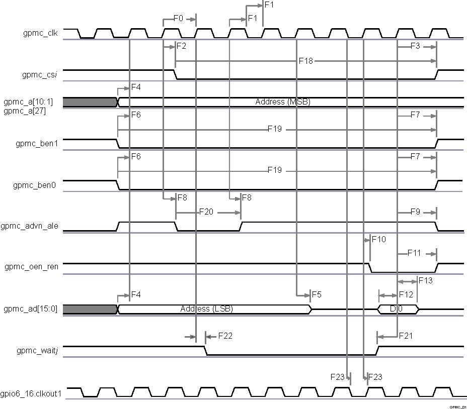 Figure 7-7 GPMC / Multiplexed 16bits NOR Flash - Synchronous Single Read -
(GpmcFCLKDivider = 0)(1)(2)
- In gpmc_csi, i = 0 to 7.
- In gpmc_waitj, j = 0 to 1.
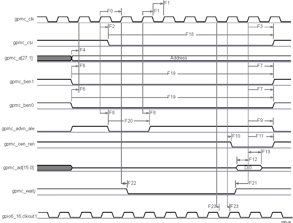 Figure 7-8 GPMC / Nonmultiplexed 16bits NOR Flash - Synchronous Single Read -
(GpmcFCLKDivider = 0)(1)(2)
- In gpmc_csi, i = 0 to 7.
- In gpmc_waitj, j = 0 to 1.
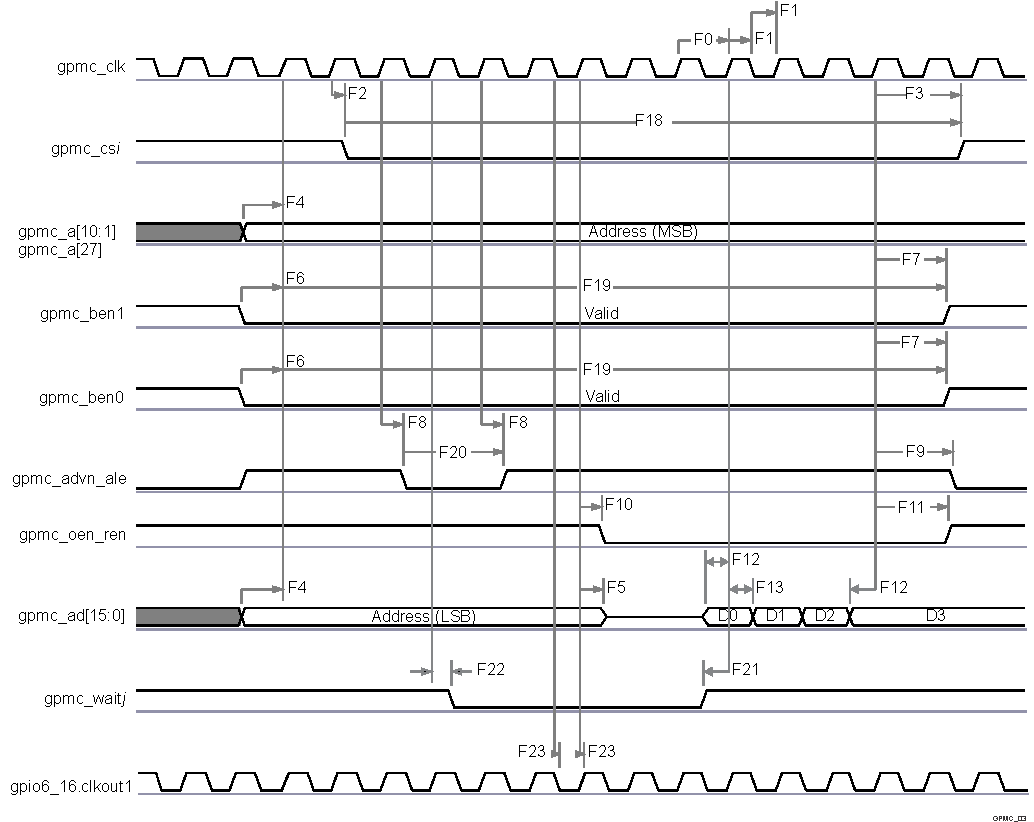 Figure 7-9 GPMC / Multiplexed 16bits NOR Flash - Synchronous Burst Read 4x16 bits -
(GpmcFCLKDivider = 0)(1)(2)
- In gpmc_csi, i= 0 to 7.
- In gpmc_waitj, j = 0 to 1.
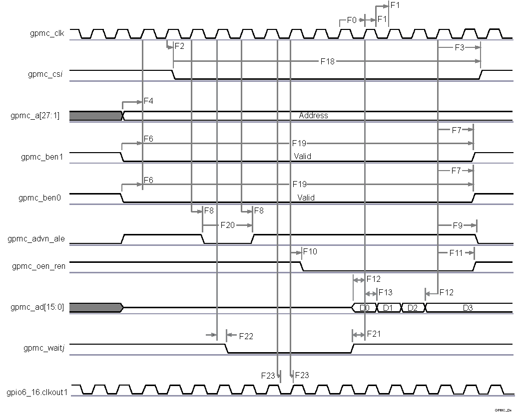 Figure 7-10 GPMC / Nonmultiplexed 16bits NOR Flash - Synchronous Burst Read 4x16 bits -
(GpmcFCLKDivider = 0)(1)(2)
- In gpmc_csi, i = 0 to 7.
- In gpmc_waitj, j = 0 to 1.
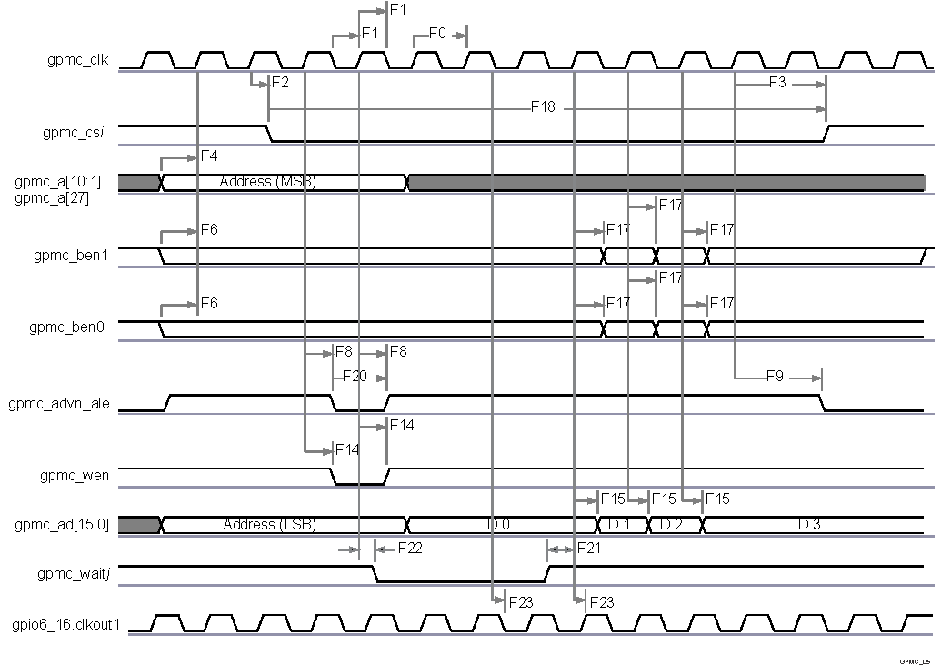 Figure 7-11 GPMC / Multiplexed 16bits NOR Flash - Synchronous Burst Write 4x16bits -
(GpmcFCLKDivider = 0)(1)(2)
- In “gpmc_csi”, i = 0 to 7.
- In “gpmc_waitj”, j = 0 to 1.
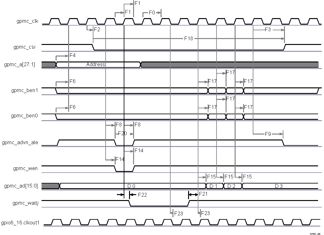 Figure 7-12 GPMC / Nonmultiplexed 16bits NOR Flash - Synchronous Burst Write 4x16bits - (GpmcFCLKDivider = 0)(1)(2)
 - In “gpmc_csi”, i = 1 to 7.
- In “gpmc_waitj”, j = 0 to 1.