ZHCSIC7H March 2016 – November 2019 DRA722 , DRA724 , DRA725 , DRA726
PRODUCTION DATA.
- 1 器件概述
- 2 修订历史记录
- 3 Device Comparison
-
4 Terminal Configuration and Functions
- 4.1 Terminal Assignment
- 4.2 Ball Characteristics
- 4.3 Multiplexing Characteristics
- 4.4
Signal Descriptions
- 4.4.1 Video Input Ports (VIP)
- 4.4.2 Display Subsystem – Video Output Ports
- 4.4.3 Display Subsystem – High-Definition Multimedia Interface (HDMI)
- 4.4.4 Camera Serial Interface 2 CAL bridge (CSI2)
- 4.4.5 External Memory Interface (EMIF)
- 4.4.6 General-Purpose Memory Controller (GPMC)
- 4.4.7 Timers
- 4.4.8 Inter-Integrated Circuit Interface (I2C)
- 4.4.9 HDQ / 1-Wire Interface (HDQ1W)
- 4.4.10 Universal Asynchronous Receiver Transmitter (UART)
- 4.4.11 Multichannel Serial Peripheral Interface (McSPI)
- 4.4.12 Quad Serial Peripheral Interface (QSPI)
- 4.4.13 Multicannel Audio Serial Port (McASP)
- 4.4.14 Universal Serial Bus (USB)
- 4.4.15 SATA
- 4.4.16 Peripheral Component Interconnect Express (PCIe)
- 4.4.17 Controller Area Network Interface (DCAN)
- 4.4.18 Ethernet Interface (GMAC_SW)
- 4.4.19 Media Local Bus (MLB) Interface
- 4.4.20 eMMC/SD/SDIO
- 4.4.21 General-Purpose Interface (GPIO)
- 4.4.22 Keyboard controller (KBD)
- 4.4.23 Pulse Width Modulation (PWM) Interface
- 4.4.24 Audio Tracking Logic (ATL)
- 4.4.25 Test Interfaces
- 4.4.26 System and Miscellaneous
- 4.4.27 Power Supplies
-
5 Specifications
- 5.1 Absolute Maximum Ratings
- 5.2 ESD Ratings
- 5.3 Power-On-Hour (POH) Limits
- 5.4 Recommended Operating Conditions
- 5.5 Operating Performance Points
- 5.6 Power Consumption Summary
- 5.7
Electrical Characteristics
- 5.7.1 LVCMOS DDR DC Electrical Characteristics
- 5.7.2 HDMIPHY DC Electrical Characteristics
- 5.7.3 Dual Voltage LVCMOS I2C DC Electrical Characteristics
- 5.7.4 IQ1833 Buffers DC Electrical Characteristics
- 5.7.5 IHHV1833 Buffers DC Electrical Characteristics
- 5.7.6 LVCMOS OSC Buffers DC Electrical Characteristics
- 5.7.7 LVCMOS CSI2 DC Electrical Characteristics
- 5.7.8 BMLB18 Buffers DC Electrical Characteristics
- 5.7.9 BC1833IHHV Buffers DC Electrical Characteristics
- 5.7.10 USBPHY DC Electrical Characteristics
- 5.7.11 Dual Voltage SDIO1833 DC Electrical Characteristics
- 5.7.12 Dual Voltage LVCMOS DC Electrical Characteristics
- 5.7.13 SATAPHY DC Electrical Characteristics
- 5.7.14 PCIEPHY DC Electrical Characteristics
- 5.8 VPP Specifications for One-Time Programmable (OTP) eFuses
- 5.9 Thermal Characteristics
- 5.10 Power Supply Sequences
- 6 Clock Specifications
-
7 Timing Requirements and Switching Characteristics
- 7.1 Timing Test Conditions
- 7.2 Interface Clock Specifications
- 7.3 Timing Parameters and Information
- 7.4 Recommended Clock and Control Signal Transition Behavior
- 7.5 Virtual and Manual I/O Timing Modes
- 7.6 Video Input Ports (VIP)
- 7.7 Display Subsystem - Video Output Ports
- 7.8 Display Subsystem - High-Definition Multimedia Interface (HDMI)
- 7.9 Camera Serial Interface 2 CAL bridge (CSI2)
- 7.10 External Memory Interface (EMIF)
- 7.11 General-Purpose Memory Controller (GPMC)
- 7.12 Timers
- 7.13 Inter-Integrated Circuit Interface (I2C)
- 7.14 HDQ / 1-Wire Interface (HDQ1W)
- 7.15 Universal Asynchronous Receiver Transmitter (UART)
- 7.16 Multichannel Serial Peripheral Interface (McSPI)
- 7.17 Quad Serial Peripheral Interface (QSPI)
- 7.18 Multichannel Audio Serial Port (McASP)
- 7.19 Universal Serial Bus (USB)
- 7.20 Serial Advanced Technology Attachment (SATA)
- 7.21 Peripheral Component Interconnect Express (PCIe)
- 7.22 Controller Area Network Interface (DCAN)
- 7.23
Ethernet Interface (GMAC_SW)
- 7.23.1
GMAC MII Timings
- Table 7-70 Timing Requirements for miin_rxclk - MII Operation
- Table 7-71 Timing Requirements for miin_txclk - MII Operation
- Table 7-72 Timing Requirements for GMAC MIIn Receive 10/100 Mbit/s
- Table 7-73 Switching Characteristics Over Recommended Operating Conditions for GMAC MIIn Transmit 10/100 Mbits/s
- 7.23.2 GMAC MDIO Interface Timings
- 7.23.3
GMAC RMII Timings
- Table 7-78 Timing Requirements for GMAC REF_CLK - RMII Operation
- Table 7-79 Timing Requirements for GMAC RMIIn Receive
- Table 7-80 Switching Characteristics Over Recommended Operating Conditions for GMAC REF_CLK - RMII Operation
- Table 7-81 Switching Characteristics Over Recommended Operating Conditions for GMAC RMIIn Transmit 10/100 Mbits/s
- 7.23.4
GMAC RGMII Timings
- Table 7-85 Timing Requirements for rgmiin_rxc - RGMIIn Operation
- Table 7-86 Timing Requirements for GMAC RGMIIn Input Receive for 10/100/1000 Mbps
- Table 7-87 Switching Characteristics Over Recommended Operating Conditions for rgmiin_txctl - RGMIIn Operation for 10/100/1000 Mbit/s
- Table 7-88 Switching Characteristics for GMAC RGMIIn Output Transmit for 10/100/1000 Mbps
- 7.23.1
GMAC MII Timings
- 7.24 Media Local Bus (MLB) interface
- 7.25
eMMC/SD/SDIO
- 7.25.1
MMC1-SD Card Interface
- 7.25.1.1 Default speed, 4-bit data, SDR, half-cycle
- 7.25.1.2 High speed, 4-bit data, SDR, half-cycle
- 7.25.1.3 SDR12, 4-bit data, half-cycle
- 7.25.1.4 SDR25, 4-bit data, half-cycle
- 7.25.1.5 UHS-I SDR50, 4-bit data, half-cycle
- 7.25.1.6 UHS-I SDR104, 4-bit data, half-cycle
- 7.25.1.7 UHS-I DDR50, 4-bit data
- 7.25.2 MMC2 - eMMC
- 7.25.3 MMC3 and MMC4-SDIO/SD
- 7.25.1
MMC1-SD Card Interface
- 7.26 General-Purpose Interface (GPIO)
- 7.27 Audio Tracking Logic (ATL)
- 7.28 System and Miscellaneous interfaces
- 7.29
Test Interfaces
- 7.29.1
IEEE 1149.1 Standard-Test-Access Port (JTAG)
- 7.29.1.1
JTAG Electrical Data/Timing
- Table 7-142 Timing Requirements for IEEE 1149.1 JTAG
- Table 7-143 Switching Characteristics Over Recommended Operating Conditions for IEEE 1149.1 JTAG
- Table 7-144 Timing Requirements for IEEE 1149.1 JTAG With RTCK
- Table 7-145 Switching Characteristics Over Recommended Operating Conditions for IEEE 1149.1 JTAG With RTCK
- 7.29.1.1
JTAG Electrical Data/Timing
- 7.29.2 Trace Port Interface Unit (TPIU)
- 7.29.1
IEEE 1149.1 Standard-Test-Access Port (JTAG)
-
8 Applications, Implementation, and Layout
- 8.1 Introduction
- 8.2 Power Optimizations
- 8.3 Core Power Domains
- 8.4 Single-Ended Interfaces
- 8.5
Differential Interfaces
- 8.5.1 General Routing Guidelines
- 8.5.2
USB 2.0 Board Design and Layout Guidelines
- 8.5.2.1 Background
- 8.5.2.2
USB PHY Layout Guide
- 8.5.2.2.1 General Routing and Placement
- 8.5.2.2.2
Specific Guidelines for USB PHY Layout
- 8.5.2.2.2.1 Analog, PLL, and Digital Power Supply Filtering
- 8.5.2.2.2.2 Analog, Digital, and PLL Partitioning
- 8.5.2.2.2.3 Board Stackup
- 8.5.2.2.2.4 Cable Connector Socket
- 8.5.2.2.2.5 Clock Routings
- 8.5.2.2.2.6 Crystals/Oscillator
- 8.5.2.2.2.7 DP/DM Trace
- 8.5.2.2.2.8 DP/DM Vias
- 8.5.2.2.2.9 Image Planes
- 8.5.2.2.2.10 Power Regulators
- 8.5.2.3 References
- 8.5.3 USB 3.0 Board Design and Layout Guidelines
- 8.5.4 HDMI Board Design and Layout Guidelines
- 8.5.5 SATA Board Design and Layout Guidelines
- 8.5.6 PCIe Board Design and Layout Guidelines
- 8.5.7 CSI2 Board Design and Routing Guidelines
- 8.6 Clock Routing Guidelines
- 8.7
DDR3 Board Design and Layout Guidelines
- 8.7.1 DDR3 General Board Layout Guidelines
- 8.7.2
DDR3 Board Design and Layout Guidelines
- 8.7.2.1 Board Designs
- 8.7.2.2 DDR3 EMIF
- 8.7.2.3 DDR3 Device Combinations
- 8.7.2.4 DDR3 Interface Schematic
- 8.7.2.5 Compatible JEDEC DDR3 Devices
- 8.7.2.6 PCB Stackup
- 8.7.2.7 Placement
- 8.7.2.8 DDR3 Keepout Region
- 8.7.2.9 Bulk Bypass Capacitors
- 8.7.2.10 High Speed Bypass Capacitors
- 8.7.2.11 Net Classes
- 8.7.2.12 DDR3 Signal Termination
- 8.7.2.13 VREF_DDR Routing
- 8.7.2.14 VTT
- 8.7.2.15 CK and ADDR_CTRL Topologies and Routing Definition
- 8.7.2.16 Data Topologies and Routing Definition
- 8.7.2.17 Routing Specification
- 9 Device and Documentation Support
- 10Mechanical, Packaging, and Orderable Information
8.2.4 Step 4: Frequency Analysis
Delivering low noise voltage sources are very important to allowing a system to operate at the lowest possible Operational Performance Point (OPP) for any one Use Case. An OPP is a combination of the supply voltage level and clocking rate for key internal processor domains. A SCH and PCB designed to provide low noise voltage supplies will then enable the processor to enter optimal OPPs for each Use Case that in turn will minimize power dissipation and junction temperatures on-die. Therefore, it is a good engineering practice to perform a Frequency Analysis over the key power domains.
Frequency analysis and design methodology results in a PDN design that minimizes transient noise voltages at the processor’s input power balls. This allows the processor’s internal transistors to operate near the minimum specified operating supply voltage levels. To accomplish this one must evaluate how a voltage supply will change due to impedance variations over frequency. This analysis will focus on the decoupling capacitor network (VDD_xxx and VSS/Gnd rails) at the load. Sufficient capacitance with a distribution of self-resonant points will provide for an overall lower impedance vs frequency response for each power domain.
Decoupling components that are distant from their load’s input power are susceptible to encountering spreading loop inductance from the PCB design. Early analysis of each key power domain’s frequency response helps to determine basic decoupling capacitor placement, optimal footprint, layer assignment, and types needed for minimizing supply voltage noise/fluctuations due to switching and load current transients.
NOTE
Evaluation of loop inductance values for decoupling capacitors placed ~300mils closer to the load’s input power balls has shown an 18% reduction in loop inductance due to reduced distance.
- Decoupling capacitors must be carefully placed in order to minimize loop inductance impact on supply voltage transients. A real capacitor has characteristics not only of capacitance but also inductance and resistance.
Figure 8-6 shows the parasitic model of a real capacitor. A real capacitor must be treated as an RLC circuit with effective series resistance (ESR) and effective series inductance (ESL).
 Figure 8-6 Characteristics of a Real Capacitor With ESL and ESR
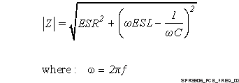
 The magnitude of the impedance of this series model is given as:
 Figure 8-7 Series Model Impedance Equation
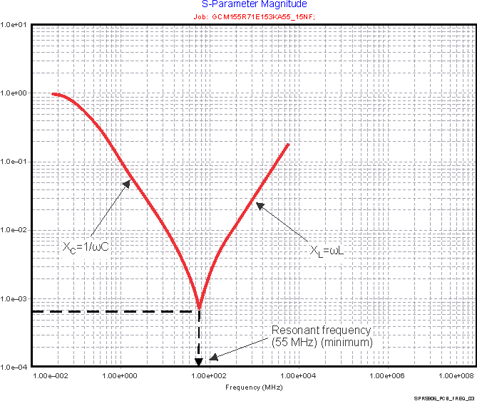
 Figure 8-8 shows the resonant frequency response of a typical capacitor with a self-resonant frequency of 55 MHz. The impedance of the capacitor is a combination of its series resistance and reactive capacitance and inductance as shown in the equation above.
 Figure 8-8 Typical Impedance Profile of a Capacitor
 Because a capacitor has series inductance and resistance that impacts its effectiveness, it is important that the following recommendations are adopted in placing capacitors on the PDN.
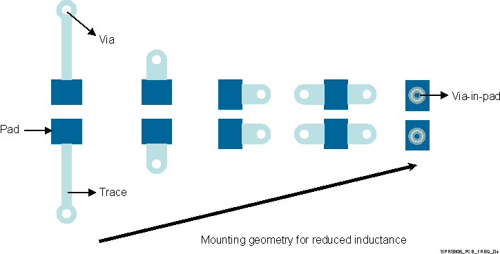
Wherever possible, mount the capacitor with the geometry that minimizes the mounting inductance and resistance. This was shown earlier in Figure 8-1. The capacitor mounting inductance and resistance values include the inductance and resistance of the pads, trace, and vias. Whenever possible, use footprints that have the lowest inductance configuration as shown in Figure 8-9
The length of a trace used to connect a capacitor has a big impact on parasitic inductance and resistance of the mounting. This trace must be as short and as wide as possible. wherever possible, minimize distance to supply and Gnd vias by locating vias nearby or within the capacitor’s solder pad landing. Further improvements can be made to the mounting by placing vias to the side of capacitor lands or doubling the number of vias as shown in Figure 8-9. If the PCB manufacturing processes allow it and if cost-effective, via-in-pad (VIP) geometries are strongly recommended.
In addition to mounting inductance and resistance associated with placing a capacitor on the PCB, the effectiveness of a decoupling capacitor also depends on the spreading inductance and resistance that the capacitor sees with respect to the load. The spreading inductance and resistance is strongly dependent on the layer assignment in the PCB stack-up. Therefore, try to minimize X, Y and Z dimensions where the Z is due to PCB thickness (as shown in Figure 8-9).
From left (highest inductance) to right (lowest inductance) the capacitor footprint types shown in Figure 8-9 are known as:
- 2-via, Skinny End Exit (2vSEE)
- 2-via, Wide End Exit (2vWEE)
- 2-via, Wide Side Exit (2vWSE)
- 4-via, Wide Side Exit (4vWSE)
- 2-via, In-Pad (2vIP)
 Figure 8-9 Capacitor Placement Geometry for Improved Mounting Inductance
 NOTE
Evaluation of loop inductance values for decoupling capacitor footprints 2vSEE (worst case) vs 4vWSE (2nd best) has shown a 30% reduction in inductance when 4vWSE footprint was used in place of 2vSEE.
Decoupling Capacitor (Dcap) Strategy:
- Use lowest inductance footprint and trace connection scheme possible for given PCB technology and layout area in order to minimize Dcap loop inductance to power pin as much as possible (see Figure 8-9).
- Place Dcaps on “same-side” as component within their power plane outline to minimize “decoupling loop inductance”. Target distance to power pin should be less than ~500mils depending upon PCB layout characteristics (plane's layer assignment and solid nature). Use PI modeling CAD tool to verify minimum inductance for top vs bottom-side placement.
- Place Dcaps on “opposite-side” as component within their power plane outline if “same-side” is not feasible or if distance to power pin is greater than ~500mils for top-side location. Use PI modeling CAD tool to verify minimum inductance for top vs bottom-side placement.
- Use minimum 10mil trace width for all voltage and gnd planes connections (that is, Dcap pads, component power pins, etc.).
- Place all voltage and gnd plane vias “as close as possible” to point of use (that is, Dcap pads, component power pins, etc.).
- Use a “Power/Gnd pad/pin to via” ratio of 1:1 whenever possible. Do not exceed 2:1 ratio for small number of vias within restricted PCB areas (that is, underneath BGA components).
Frequency analysis for the CORE power domain has yielded the vdd Impedance vs Frequency response shown in Section 8.3.8.2, vdd Example Analysis. As the example shows the overall CORE PDN Reff meets the maximum recommended PDN resistance of 10mΩ.