ZHCSJ46F December 2016 – December 2018 DRA74P , DRA75P
ADVANCE INFORMATION for pre-production products; subject to change without notice.
- 1器件概述
- 2修订历史记录
- 3Device Comparison
-
4Terminal Configuration and Functions
- 4.1 Pin Diagram
- 4.2 Pin Attributes
- 4.3
Signal Descriptions
- 4.3.1 VIP
- 4.3.2 DSS
- 4.3.3 HDMI
- 4.3.4 EMIF
- 4.3.5 GPMC
- 4.3.6 Timers
- 4.3.7 I2C
- 4.3.8 HDQ1W
- 4.3.9 UART
- 4.3.10 McSPI
- 4.3.11 QSPI
- 4.3.12 McASP
- 4.3.13 USB
- 4.3.14 SATA
- 4.3.15 PCIe
- 4.3.16 DCAN and MCAN
- 4.3.17 GMAC_SW
- 4.3.18 MLB
- 4.3.19 eMMC/SD/SDIO
- 4.3.20 GPIO
- 4.3.21 KBD
- 4.3.22 PWM
- 4.3.23 ATL
- 4.3.24 Test Interfaces
- 4.3.25 System and Miscellaneous
- 4.4 Pin Multiplexing
- 4.5 Connections for Unused Pins
-
5Specifications
- 5.1 Absolute Maximum Ratings
- 5.2 ESD Ratings
- 5.3 Power-On Hours (POH)
- 5.4 Recommended Operating Conditions
- 5.5 Operating Performance Points
- 5.6 Power Consumption Summary
- 5.7
Electrical Characteristics
- Table 5-6 LVCMOS DDR DC Electrical Characteristics
- Table 5-7 Dual Voltage LVCMOS I2C DC Electrical Characteristics
- Table 5-8 IQ1833 Buffers DC Electrical Characteristics
- Table 5-9 IHHV1833 Buffers DC Electrical Characteristics
- Table 5-10 LVCMOS OSC Buffers DC Electrical Characteristics
- Table 5-11 BMLB18 Buffers DC Electrical Characteristics
- Table 5-12 BC1833IHHV Buffers DC Electrical Characteristics
- Table 5-13 Dual Voltage SDIO1833 DC Electrical Characteristics
- Table 5-14 Dual Voltage LVCMOS DC Electrical Characteristics
- 5.7.1 HDMIPHY DC Electrical Characteristics
- 5.7.2 USBPHY DC Electrical Characteristics
- 5.7.3 SATAPHY DC Electrical Characteristics
- 5.7.4 PCIEPHY DC Electrical Characteristics
- 5.8 VPP Specifications for One-Time Programmable (OTP) eFuses
- 5.9 Thermal Resistance Characteristics
- 5.10
Timing Requirements and Switching Characteristics
- 5.10.1 Timing Parameters and Information
- 5.10.2 Interface Clock Specifications
- 5.10.3 Power Supply Sequences
- 5.10.4 Clock Specifications
- 5.10.5 Recommended Clock and Control Signal Transition Behavior
- 5.10.6
Peripherals
- 5.10.6.1 Timing Test Conditions
- 5.10.6.2 Virtual and Manual I/O Timing Modes
- 5.10.6.3 VIP
- 5.10.6.4 DSS
- 5.10.6.5 HDMI
- 5.10.6.6 EMIF
- 5.10.6.7 GPMC
- 5.10.6.8 Timers
- 5.10.6.9 I2C
- 5.10.6.10 HDQ1W
- 5.10.6.11 UART
- 5.10.6.12 McSPI
- 5.10.6.13 QSPI
- 5.10.6.14
McASP
- Table 5-79 Timing Requirements for McASP1
- Table 5-80 Timing Requirements for McASP2
- Table 5-81 Timing Requirements for McASP3/4/5/6/7/8
- Table 5-82 Switching Characteristics Over Recommended Operating Conditions for McASP1
- Table 5-83 Switching Characteristics Over Recommended Operating Conditions for McASP2
- Table 5-84 Switching Characteristics Over Recommended Operating Conditions for McASP3/4/5/6/7/8
- 5.10.6.15 USB
- 5.10.6.16 SATA
- 5.10.6.17 PCIe
- 5.10.6.18 CAN
- 5.10.6.19
GMAC_SW
- 5.10.6.19.1
GMAC MII Timings
- Table 5-101 Timing Requirements for miin_rxclk - MII Operation
- Table 5-102 Timing Requirements for miin_txclk - MII Operation
- Table 5-103 Timing Requirements for GMAC MIIn Receive 10/100 Mbit/s
- Table 5-104 Switching Characteristics Over Recommended Operating Conditions for GMAC MIIn Transmit 10/100 Mbits/s
- 5.10.6.19.2 GMAC MDIO Interface Timings
- 5.10.6.19.3
GMAC RMII Timings
- Table 5-109 Timing Requirements for GMAC REF_CLK - RMII Operation
- Table 5-110 Timing Requirements for GMAC RMIIn Receive
- Table 5-111 Switching Characteristics Over Recommended Operating Conditions for GMAC REF_CLK - RMII Operation
- Table 5-112 Switching Characteristics Over Recommended Operating Conditions for GMAC RMIIn Transmit 10/100 Mbits/s
- 5.10.6.19.4
GMAC RGMII Timings
- Table 5-116 Timing Requirements for rgmiin_rxc - RGMIIn Operation
- Table 5-117 Timing Requirements for GMAC RGMIIn Input Receive for 10/100/1000 Mbps
- Table 5-118 Switching Characteristics Over Recommended Operating Conditions for rgmiin_txctl - RGMIIn Operation for 10/100/1000 Mbit/s
- Table 5-119 Switching Characteristics for GMAC RGMIIn Output Transmit for 10/100/1000 Mbps
- 5.10.6.19.1
GMAC MII Timings
- 5.10.6.20 MLB
- 5.10.6.21
eMMC/SD/SDIO
- 5.10.6.21.1
MMC1—SD Card Interface
- 5.10.6.21.1.1 Default speed, 4-bit data, SDR, half-cycle
- 5.10.6.21.1.2 High speed, 4-bit data, SDR, half-cycle
- 5.10.6.21.1.3 SDR12, 4-bit data, half-cycle
- 5.10.6.21.1.4 SDR25, 4-bit data, half-cycle
- 5.10.6.21.1.5 UHS-I SDR50, 4-bit data, half-cycle
- 5.10.6.21.1.6 UHS-I SDR104, 4-bit data, half-cycle
- 5.10.6.21.1.7 UHS-I DDR50, 4-bit data
- 5.10.6.21.2 MMC2 — eMMC
- 5.10.6.21.3 MMC3 and MMC4—SDIO/SD
- 5.10.6.21.1
MMC1—SD Card Interface
- 5.10.6.22 GPIO
- 5.10.6.23 ATL
- 5.10.6.24 System and Miscellaneous Interfaces
- 5.10.7
Emulation and Debug Subsystem
- 5.10.7.1
JTAG
- 5.10.7.1.1
JTAG Electrical Data/Timing
- Table 5-176 Timing Requirements for IEEE 1149.1 JTAG
- Table 5-177 Switching Characteristics Over Recommended Operating Conditions for IEEE 1149.1 JTAG
- Table 5-178 Timing Requirements for IEEE 1149.1 JTAG With RTCK
- Table 5-179 Switching Characteristics Over Recommended Operating Conditions for IEEE 1149.1 JTAG With RTCK
- 5.10.7.1.1
JTAG Electrical Data/Timing
- 5.10.7.2 TPIU
- 5.10.7.1
JTAG
-
6Detailed Description
- 6.1 Description
- 6.2 Functional Block Diagram
- 6.3 MPU
- 6.4 DSP Subsystem
- 6.5 ISS
- 6.6 IVA
- 6.7 EVE
- 6.8 IPU
- 6.9 VPE
- 6.10 GPU
- 6.11 ATL Overview
- 6.12 Memory Subsystem
- 6.13 Interprocessor Communication
- 6.14 Interrupt Controller
- 6.15 EDMA
- 6.16 Peripherals
- 6.17 On-Chip Debug
-
7Applications, Implementation, and Layout
- 7.1 Introduction
- 7.2 Power Optimizations
- 7.3 Core Power Domains
- 7.4 Single-Ended Interfaces
- 7.5
Differential Interfaces
- 7.5.1 General Routing Guidelines
- 7.5.2
USB 2.0 Board Design and Layout Guidelines
- 7.5.2.1 Background
- 7.5.2.2
USB PHY Layout Guide
- 7.5.2.2.1 General Routing and Placement
- 7.5.2.2.2
Specific Guidelines for USB PHY Layout
- 7.5.2.2.2.1 Analog, PLL, and Digital Power Supply Filtering
- 7.5.2.2.2.2 Analog, Digital, and PLL Partitioning
- 7.5.2.2.2.3 Board Stackup
- 7.5.2.2.2.4 Cable Connector Socket
- 7.5.2.2.2.5 Clock Routings
- 7.5.2.2.2.6 Crystals/Oscillator
- 7.5.2.2.2.7 DP/DM Trace
- 7.5.2.2.2.8 DP/DM Vias
- 7.5.2.2.2.9 Image Planes
- 7.5.2.2.2.10 JTAG Interface
- 7.5.2.2.2.11 Power Regulators
- 7.5.2.3 Electrostatic Discharge (ESD)
- 7.5.2.4 References
- 7.5.3 USB 3.0 Board Design and Layout Guidelines
- 7.5.4 HDMI Board Design and Layout Guidelines
- 7.5.5 SATA Board Design and Layout Guidelines
- 7.5.6 PCIe Board Design and Layout Guidelines
- 7.6 Clock Routing Guidelines
- 7.7
DDR2/DDR3 Board Design and Layout Guidelines
- 7.7.1 DDR2/DDR3 General Board Layout Guidelines
- 7.7.2 DDR2 Board Design and Layout Guidelines
- 7.7.3
DDR3 Board Design and Layout Guidelines
- 7.7.3.1 Board Designs
- 7.7.3.2 DDR3 EMIF
- 7.7.3.3 DDR3 Device Combinations
- 7.7.3.4 DDR3 Interface Schematic
- 7.7.3.5 Compatible JEDEC DDR3 Devices
- 7.7.3.6 PCB Stackup
- 7.7.3.7 Placement
- 7.7.3.8 DDR3 Keepout Region
- 7.7.3.9 Bulk Bypass Capacitors
- 7.7.3.10 High-Speed Bypass Capacitors
- 7.7.3.11 Net Classes
- 7.7.3.12 DDR3 Signal Termination
- 7.7.3.13 VREF_DDR Routing
- 7.7.3.14 VTT
- 7.7.3.15 CK and ADDR_CTRL Topologies and Routing Definition
- 7.7.3.16 Data Topologies and Routing Definition
- 7.7.3.17 Routing Specification
- 8Device and Documentation Support
- 9Mechanical Packaging and Orderable Information
5.10.6.7.1 GPMC/NOR Flash Interface Synchronous Timing
CAUTION
The IO Timings provided in this section are only valid for some GPMC usage modes when the corresponding Virtual IO Timings or Manual IO Timings are configured as described in the tables found in this section.
Table 5-55 and Table 5-56 assume testing over the recommended operating conditions and electrical characteristic conditions below (see Figure 5-28, Figure 5-29, Figure 5-30, Figure 5-31, Figure 5-32, and Figure 5-33).
Table 5-55 GPMC/NOR Flash Interface Timing Requirements - Synchronous Mode - Default
| NO. | PARAMETER | DESCRIPTION | MIN | MAX | UNIT |
|---|---|---|---|---|---|
| F12 | tsu(dV-clkH) | Setup time, read gpmc_ad[15:0] valid before gpmc_clk high | 1.9 | ns | |
| F13 | th(clkH-dV) | Hold time, read gpmc_ad[15:0] valid after gpmc_clk high | 1 | ns | |
| F21 | tsu(waitV-clkH) | Setup time, gpmc_wait[1:0] valid before gpmc_clk high | 1.9 | ns | |
| F22 | th(clkH-waitV) | Hold Time, gpmc_wait[1:0] valid after gpmc_clk high | 1 | ns |
NOTE
Wait monitoring support is limited to a WaitMonitoringTime value > 0. For a full description of wait monitoring feature, see General-Purpose Memory Controller section in the Device TRM.
Table 5-56 GPMC/NOR Flash Interface Switching Characteristics - Synchronous Mode - Default
| NO. | PARAMETER | DESCRIPTION | MIN | MAX | UNIT |
|---|---|---|---|---|---|
| F0 | tc(clk) | Cycle time, output clock gpmc_clk period (12) | 11.3 | ns | |
| F2 | td(clkH-nCSV) | Delay time, gpmc_clk rising edge to gpmc_cs[7:0] transition (14) | F-0.8 (6) | F+3.17 (6) | ns |
| F3 | td(clkH-nCSIV) | Delay time, gpmc_clk rising edge to gpmc_cs[7:0] invalid (14) | E-0.8 (5) | E+3.1 (5) | ns |
| F4 | td(ADDV-clk) | Delay time, gpmc_a[27:0] address bus valid to gpmc_clk first edge | B-0.8 (2) | B+3.43 (2) | ns |
| F5 | td(clkH-ADDIV) | Delay time, gpmc_clk rising edge to gpmc_a[27:0] gpmc address bus invalid | -0.8 | ns | |
| F6 | td(nBEV-clk) | Delay time, gpmc_ben[1:0] valid to gpmc_clk rising edge | B-3.8 | B+2.37 | ns |
| F7 | td(clkH-nBEIV) | Delay time, gpmc_clk rising edge to gpmc_ben[1:0] invalid | D-0.4 | D+1.1 | ns |
| F8 | td(clkH-nADV) | Delay time, gpmc_clk rising edge to gpmc_advn_ale transition (14) | G-0.8 (7) | G+3.1 (7) | ns |
| F9 | td(clkH-nADVIV) | Delay time, gpmc_clk rising edge to gpmc_advn_ale invalid (14) | D-0.8 (4) | D+3.1 (4) | ns |
| F10 | td(clkH-nOE) | Delay time, gpmc_clk rising edge to gpmc_oen_ren transition (14) | H-0.8 (8) | H+2.45 (8) | ns |
| F11 | td(clkH-nOEIV) | Delay time, gpmc_clk rising edge to gpmc_oen_ren invalid (14) | E-0.8 (5) | E+2.1 (5) | ns |
| F14 | td(clkH-nWE) | Delay time, gpmc_clk rising edge to gpmc_wen transition (14) | I-0.8 (9) | I+3.1 (9) | ns |
| F15 | td(clkH-Data) | Delay time, gpmc_clk rising edge to gpmc_ad[15:0] data bus transition | J-1.1 (10) | J+4.89 (10) | ns |
| F17 | td(clkH-nBE) | Delay time, gpmc_clk rising edge to gpmc_ben[1:0] transition | J-1.1 (10) | J+3.8 (10) | ns |
| F18 | tw(nCSV) | Pulse duration, gpmc_cs[7:0] low | A (1) | ns | |
| F19 | tw(nBEV) | Pulse duration, gpmc_ben[1:0] low | C (3) | ns | |
| F20 | tw(nADVV) | Pulse duration, gpmc_advn_ale low | K (11) | ns | |
| F23 | td(CLK-GPIO) | Delay time, gpmc_clk transition to gpio6_16 transition (13) | 1.2 | 6.1 | ns |
Table 5-57 GPMC/NOR Flash Interface Timing Requirements - Synchronous Mode - Alternate
| NO. | PARAMETER | DESCRIPTION | MIN | MAX | UNIT |
|---|---|---|---|---|---|
| F12 | tsu(dV-clkH) | Setup time, read gpmc_ad[15:0] valid before gpmc_clk high | 2.5 | ns | |
| F13 | th(clkH-dV) | Hold time, read gpmc_ad[15:0] valid after gpmc_clk high | 1.9 | ns | |
| F21 | tsu(waitV-clkH) | Setup time, gpmc_wait[1:0] valid before gpmc_clk high | 2.5 | ns | |
| F22 | th(clkH-waitV) | Hold Time, gpmc_wait[1:0] valid after gpmc_clk high | 1.9 | ns |
Table 5-58 GPMC/NOR Flash Interface Switching Characteristics - Synchronous Mode - Alternate
| NO. | PARAMETER | DESCRIPTION | MIN | MAX | UNIT |
|---|---|---|---|---|---|
| F0 | tc(clk) | Cycle time, output clock gpmc_clk period (12) | 15.04 | ns | |
| F2 | td(clkH-nCSV) | Delay time, gpmc_clk rising edge to gpmc_cs[7:0] transition (14) | F-0.13 (6) | F+6.1 (6) | ns |
| F3 | td(clkH-nCSIV) | Delay time, gpmc_clk rising edge to gpmc_cs[7:0] invalid (14) | E+0.7 (5) | E+6.1 (5) | ns |
| F4 | td(ADDV-clk) | Delay time, gpmc_a[27:0] address bus valid to gpmc_clk first edge | B+0.21 (2) | B+6.1 (2) | ns |
| F5 | td(clkH-ADDIV) | Delay time, gpmc_clk rising edge to gpmc_a[27:0] gpmc address bus invalid | 0.7 | ns | |
| F6 | td(nBEV-clk) | Delay time, gpmc_ben[1:0] valid to gpmc_clk rising edge | B-4.9 | B+0.4 | ns |
| F7 | td(clkH-nBEIV) | Delay time, gpmc_clk rising edge to gpmc_ben[1:0] invalid | D-0.4 | D+4.9 | ns |
| F8 | td(clkH-nADV) | Delay time, gpmc_clk rising edge to gpmc_advn_ale transition (14) | G+0.7 (7) | G+6.1 (7) | ns |
| F9 | td(clkH-nADVIV) | Delay time, gpmc_clk rising edge to gpmc_advn_ale invalid (14) | D+0.7 (4) | D+6.1 (4) | ns |
| F10 | td(clkH-nOE) | Delay time, gpmc_clk rising edge to gpmc_oen_ren transition (14) | H+0.42 (8) | H+5.1 (8) | ns |
| F11 | td(clkH-nOEIV) | Delay time, gpmc_clk rising edge to gpmc_oen_ren invalid (14) | E+0.7 (5) | E+5.1 (5) | ns |
| F14 | td(clkH-nWE) | Delay time, gpmc_clk rising edge to gpmc_wen transition (14) | I+0.46 (9) | I+6.1 (9) | ns |
| F15 | td(clkH-Data) | Delay time, gpmc_clk rising edge to gpmc_ad[15:0] data bus transition | J-0.4 (10) | J+4.9 (10) | ns |
| F17 | td(clkH-nBE) | Delay time, gpmc_clk rising edge to gpmc_ben[1:0] transition | J-0.4 (10) | J+5.63 (10) | ns |
| F18 | tw(nCSV) | Pulse duration, gpmc_cs[7:0] low | A (1) | ns | |
| F19 | tw(nBEV) | Pulse duration, gpmc_ben[1:0] low | C (3) | ns | |
| F20 | tw(nADVV) | Pulse duration, gpmc_advn_ale low | K (11) | ns | |
| F23 | td(CLK-GPIO) | Delay time, gpmc_clk transition to gpio6_16 transition (13) | 0.96 | 6.1 | ns |
- For single read: A = (CSRdOffTime - CSOnTime) × (TimeParaGranularity + 1) × GPMC_FCLK period
For burst read: A = (CSRdOffTime - CSOnTime + (n - 1) × PageBurstAccessTime) × (TimeParaGranularity + 1) × GPMC_FCLK period
For burst write: A = (CSWrOffTime - CSOnTime + (n - 1) × PageBurstAccessTime) × (TimeParaGranularity + 1) × GPMC_FCLK period with n the page burst access number. - B = ClkActivationTime × GPMC_FCLK
- For single read: C = RdCycleTime × (TimeParaGranularity + 1) × GPMC_FCLK
For burst read: C = (RdCycleTime + (n – 1) × PageBurstAccessTime) × (TimeParaGranularity + 1) × GPMC_FCLK
For Burst write: C = (WrCycleTime + (n – 1) × PageBurstAccessTime) × (TimeParaGranularity + 1) × GPMC_FCLK with n the page burst access number. - For single read: D = (RdCycleTime – AccessTime) × (TimeParaGranularity + 1) × GPMC_FCLK
For burst read: D = (RdCycleTime – AccessTime) × (TimeParaGranularity + 1) × GPMC_FCLK
For burst write: D = (WrCycleTime – AccessTime) × (TimeParaGranularity + 1) × GPMC_FCLK - For single read: E = (CSRdOffTime – AccessTime) × (TimeParaGranularity + 1) × GPMC_FCLK
For burst read: E = (CSRdOffTime – AccessTime) × (TimeParaGranularity + 1) × GPMC_FCLK
For burst write: E = (CSWrOffTime – AccessTime) × (TimeParaGranularity + 1) × GPMC_FCLK - For nCS falling edge (CS activated):
Case GpmcFCLKDivider = 0 :
F = 0.5 × CSExtraDelay × GPMC_FCLK Case GpmcFCLKDivider = 1:
F = 0.5 × CSExtraDelay × GPMC_FCLK if (ClkActivationTime and CSOnTime are odd) or (ClkActivationTime and CSOnTime are even)
F = (1 + 0.5 × CSExtraDelay) × GPMC_FCLK otherwise
Case GpmcFCLKDivider = 2:
F = 0.5 × CSExtraDelay × GPMC_FCLK if ((CSOnTime – ClkActivationTime) is a multiple of 3)
F = (1 + 0.5 × CSExtraDelay) × GPMC_FCLK if ((CSOnTime – ClkActivationTime – 1) is a multiple of 3)
F = (2 + 0.5 × CSExtraDelay) × GPMC_FCLK if ((CSOnTime – ClkActivationTime – 2) is a multiple of 3)
Case GpmcFCLKDivider = 3:
F = 0.5 × CSExtraDelay × GPMC_FCLK if ((CSOnTime - ClkActivationTime) is a multiple of 4)
F = (1 + 0.5 × CSExtraDelay) × GPMC_FCLK if ((CSOnTime - ClkActivationTime - 1) is a multiple of 4)
F = (2 + 0.5 × CSExtraDelay) × GPMC_FCLK if ((CSOnTime - ClkActivationTime - 2) is a multiple of 4)
F = (3 + 0.5 × CSExtraDelay) × GPMC_FCLK if ((CSOnTime - ClkActivationTime - 3) is a multiple of 4) - For ADV falling edge (ADV activated):
Case GpmcFCLKDivider = 0 :
G = 0.5 × ADVExtraDelay × GPMC_FCLK
Case GpmcFCLKDivider = 1:
G = 0.5 × ADVExtraDelay × GPMC_FCLK if (ClkActivationTime and ADVOnTime are odd) or (ClkActivationTime and ADVOnTime are even)
G = (1 + 0.5 × ADVExtraDelay) × GPMC_FCLK otherwise
Case GpmcFCLKDivider = 2:
G = 0.5 × ADVExtraDelay × GPMC_FCLK if ((ADVOnTime – ClkActivationTime) is a multiple of 3)
G = (1 + 0.5 × ADVExtraDelay) × GPMC_FCLK if ((ADVOnTime – ClkActivationTime – 1) is a multiple of 3)
G = (2 + 0.5 × ADVExtraDelay) × GPMC_FCLK if ((ADVOnTime – ClkActivationTime – 2) is a multiple of 3)
For ADV rising edge (ADV deactivated) in Reading mode:
Case GpmcFCLKDivider = 0:
G = 0.5 × ADVExtraDelay × GPMC_FCLK
Case GpmcFCLKDivider = 1:
G = 0.5 × ADVExtraDelay × GPMC_FCLK if (ClkActivationTime and ADVRdOffTime are odd) or (ClkActivationTime and ADVRdOffTime are even)
G = (1 + 0.5 × ADVExtraDelay) × GPMC_FCLK otherwise
Case GpmcFCLKDivider = 2:
G = 0.5 × ADVExtraDelay × GPMC_FCLK if ((ADVRdOffTime – ClkActivationTime) is a multiple of 3)
G = (1 + 0.5 × ADVExtraDelay) × GPMC_FCLK if ((ADVRdOffTime – ClkActivationTime – 1) is a multiple of 3)
G = (2 + 0.5 × ADVExtraDelay) × GPMC_FCLK if ((ADVRdOffTime – ClkActivationTime – 2) is a multiple of 3)
Case GpmcFCLKDivider = 3:
G = 0.5 × ADVExtraDelay × GPMC_FCLK if ((ADVRdOffTime – ClkActivationTime) is a multiple of 4)
G = (1 + 0.5 × ADVExtraDelay) × GPMC_FCLK if ((ADVRdOffTime – ClkActivationTime – 1) is a multiple of 4)
G = (2 + 0.5 × ADVExtraDelay) × GPMC_FCLK if ((ADVRdOffTime – ClkActivationTime – 2) is a multiple of 4)
G = (3 + 0.5 × ADVExtraDelay) × GPMC_FCLK if ((ADVRdOffTime – ClkActivationTime – 3) is a multiple of 4)
For ADV rising edge (ADV deactivated) in Writing mode:
Case GpmcFCLKDivider = 0:
G = 0.5 × ADVExtraDelay × GPMC_FCLK
Case GpmcFCLKDivider = 1:
G = 0.5 × ADVExtraDelay × GPMC_FCLK if (ClkActivationTime and ADVWrOffTime are odd) or (ClkActivationTime and ADVWrOffTime are even)
G = (1 + 0.5 × ADVExtraDelay) × GPMC_FCLK otherwise
Case GpmcFCLKDivider = 2:
G = 0.5 × ADVExtraDelay × GPMC_FCLK if ((ADVWrOffTime – ClkActivationTime) is a multiple of 3)
G = (1 + 0.5 × ADVExtraDelay) × GPMC_FCLK if ((ADVWrOffTime – ClkActivationTime – 1) is a multiple of 3)
G = (2 + 0.5 × ADVExtraDelay) × GPMC_FCLK if ((ADVWrOffTime – ClkActivationTime – 2) is a multiple of 3)
Case GpmcFCLKDivider = 3:
G = 0.5 × ADVExtraDelay × GPMC_FCLK if ((ADVWrOffTime – ClkActivationTime) is a multiple of 4)
G = (1 + 0.5 × ADVExtraDelay) × GPMC_FCLK if ((ADVWrOffTime – ClkActivationTime – 1) is a multiple of 4)
G = (2 + 0.5 × ADVExtraDelay) × GPMC_FCLK if ((ADVWrOffTime – ClkActivationTime – 2) is a multiple of 4)
G = (3 + 0.5 × ADVExtraDelay) × GPMC_FCLK if ((ADVWrOffTime – ClkActivationTime – 3) is a multiple of 4) - For OE falling edge (OE activated):
Case GpmcFCLKDivider = 0:
- H = 0.5 × OEExtraDelay × GPMC_FCLK
Case GpmcFCLKDivider = 1:
- H = 0.5 × OEExtraDelay × GPMC_FCLK if (ClkActivationTime and OEOnTime are odd) or (ClkActivationTime and OEOnTime are even)
- H = (1 + 0.5 × OEExtraDelay) × GPMC_FCLK otherwise
Case GpmcFCLKDivider = 2:
- H = 0.5 × OEExtraDelay × GPMC_FCLK if ((OEOnTime – ClkActivationTime) is a multiple of 3)
- H = (1 + 0.5 × OEExtraDelay) × GPMC_FCLK if ((OEOnTime – ClkActivationTime – 1) is a multiple of 3)
- H = (2 + 0.5 × OEExtraDelay) × GPMC_FCLK if ((OEOnTime – ClkActivationTime – 2) is a multiple of 3)
Case GpmcFCLKDivider = 3:
- H = 0.5 × OEExtraDelay × GPMC_FCLK if ((OEOnTime - ClkActivationTime) is a multiple of 4)
- H = (1 + 0.5 × OEExtraDelay) × GPMC_FCLK if ((OEOnTime - ClkActivationTime - 1) is a multiple of 4)
- H = (2 + 0.5 × OEExtraDelay) × GPMC_FCLK if ((OEOnTime - ClkActivationTime - 2) is a multiple of 4)
- H = (3 + 0.5 × OEExtraDelay)) × GPMC_FCLK if ((OEOnTime - ClkActivationTime - 3) is a multiple of 4)
For OE rising edge (OE deactivated):
Case GpmcFCLKDivider = 0:
- H = 0.5 × OEExtraDelay × GPMC_FCLK
Case GpmcFCLKDivider = 1:
- H = 0.5 × OEExtraDelay × GPMC_FCLK if (ClkActivationTime and OEOffTime are odd) or (ClkActivationTime and OEOffTime are even)
- H = (1 + 0.5 × OEExtraDelay) × GPMC_FCLK otherwise
Case GpmcFCLKDivider = 2:
- H = 0.5 × OEExtraDelay × GPMC_FCLK if ((OEOffTime – ClkActivationTime) is a multiple of 3)
- H = (1 + 0.5 × OEExtraDelay) × GPMC_FCLK if ((OEOffTime – ClkActivationTime – 1) is a multiple of 3)
- H = (2 + 0.5 × OEExtraDelay) × GPMC_FCLK if ((OEOffTime – ClkActivationTime – 2) is a multiple of 3)
Case GpmcFCLKDivider = 3:
- H = 0.5 × OEExtraDelay × GPMC_FCLK if ((OEOffTime – ClkActivationTime) is a multiple of 4)
- H = (1 + 0.5 × OEExtraDelay) × GPMC_FCLK if ((OEOffTime – ClkActivationTime – 1) is a multiple of 4)
- H = (2 + 0.5 × OEExtraDelay) × GPMC_FCLK if ((OEOffTime – ClkActivationTime – 2) is a multiple of 4)
- H = (3 + 0.5 × OEExtraDelay) × GPMC_FCLK if ((OEOffTime – ClkActivationTime – 3) is a multiple of 4) - For WE falling edge (WE activated):
Case GpmcFCLKDivider = 0:
- I = 0.5 × WEExtraDelay × GPMC_FCLK
Case GpmcFCLKDivider = 1:
- I = 0.5 × WEExtraDelay × GPMC_FCLK if (ClkActivationTime and WEOnTime are odd) or (ClkActivationTime and WEOnTime are even)
- I = (1 + 0.5 × WEExtraDelay) × GPMC_FCLK otherwise
Case GpmcFCLKDivider = 2:
- I = 0.5 × WEExtraDelay × GPMC_FCLK if ((WEOnTime – ClkActivationTime) is a multiple of 3)
- I = (1 + 0.5 × WEExtraDelay) × GPMC_FCLK if ((WEOnTime – ClkActivationTime – 1) is a multiple of 3)
- I = (2 + 0.5 × WEExtraDelay) × GPMC_FCLK if ((WEOnTime – ClkActivationTime – 2) is a multiple of 3)
Case GpmcFCLKDivider = 3:
- I = 0.5 × WEExtraDelay × GPMC_FCLK if ((WEOnTime - ClkActivationTime) is a multiple of 4)
- I = (1 + 0.5 × WEExtraDelay) × GPMC_FCLK if ((WEOnTime - ClkActivationTime - 1) is a multiple of 4)
- I = (2 + 0.5 × WEExtraDelay) × GPMC_FCLK if ((WEOnTime - ClkActivationTime - 2) is a multiple of 4)
- I = (3 + 0.5 × WEExtraDelay) × GPMC_FCLK if ((WEOnTime - ClkActivationTime - 3) is a multiple of 4)
For WE rising edge (WE deactivated):
Case GpmcFCLKDivider = 0:
- I = 0.5 × WEExtraDelay × GPMC_FCLK
Case GpmcFCLKDivider = 1:
- I = 0.5 × WEExtraDelay × GPMC_FCLK if (ClkActivationTime and WEOffTime are odd) or (ClkActivationTime and WEOffTime are even)
- I = (1 + 0.5 × WEExtraDelay) × GPMC_FCLK otherwise
Case GpmcFCLKDivider = 2:
- I = 0.5 × WEExtraDelay × GPMC_FCLK if ((WEOffTime – ClkActivationTime) is a multiple of 3)
- I = (1 + 0.5 × WEExtraDelay) × GPMC_FCLK if ((WEOffTime – ClkActivationTime – 1) is a multiple of 3)
- I = (2 + 0.5 × WEExtraDelay) × GPMC_FCLK if ((WEOffTime – ClkActivationTime – 2) is a multiple of 3)
Case GpmcFCLKDivider = 3:
- I = 0.5 × WEExtraDelay × GPMC_FCLK if ((WEOffTime - ClkActivationTime) is a multiple of 4)
- I = (1 + 0.5 × WEExtraDelay) × GPMC_FCLK if ((WEOffTime - ClkActivationTime - 1) is a multiple of 4)
- I = (2 + 0.5 × WEExtraDelay) × GPMC_FCLK if ((WEOffTime - ClkActivationTime - 2) is a multiple of 4)
- I = (3 + 0.5 × WEExtraDelay) × GPMC_FCLK if ((WEOffTime - ClkActivationTime - 3) is a multiple of 4) - J = GPMC_FCLK period, where GPMC_FCLK is the General Purpose Memory Controller internal functional clock
- For read:
K = (ADVRdOffTime – ADVOnTime) × (TimeParaGranularity + 1) × GPMC_FCLK
For write: K = (ADVWrOffTime – ADVOnTime) × (TimeParaGranularity + 1) × GPMC_FCLK - The gpmc_clk output clock maximum and minimum frequency is programmable in the I/F module by setting the GPMC_CONFIG1_CSx configuration register bit fields GpmcFCLKDivider
- gpio6_16 programmed to MUXMODE=9 (clkout1), CM_CLKSEL_CLKOUTMUX1 programmed to 7 (CORE_DPLL_OUT_DCLK), CM_CLKSEL_CORE_DPLL_OUT_CLK_CLKOUTMUX programmed to 1.
- CSEXTRADELAY = 0, ADVEXTRADELAY = 0, WEEXTRADELAY = 0, OEEXTRADELAY = 0. Extra half-GPMC_FCLK cycle delay mode is not timed.
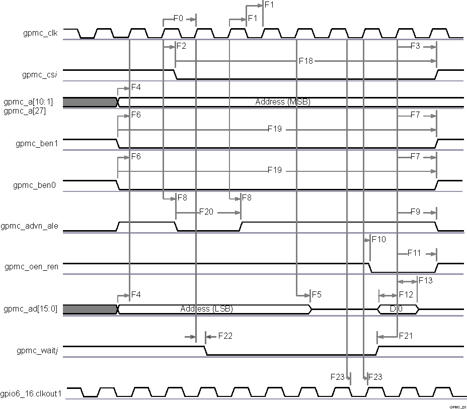 Figure 5-28 GPMC / Multiplexed 16bits NOR Flash - Synchronous Single Read -
(GpmcFCLKDivider = 0)(1)(2)
- In gpmc_csi, i = 0 to 7.
- In gpmc_waitj, j = 0 to 1.
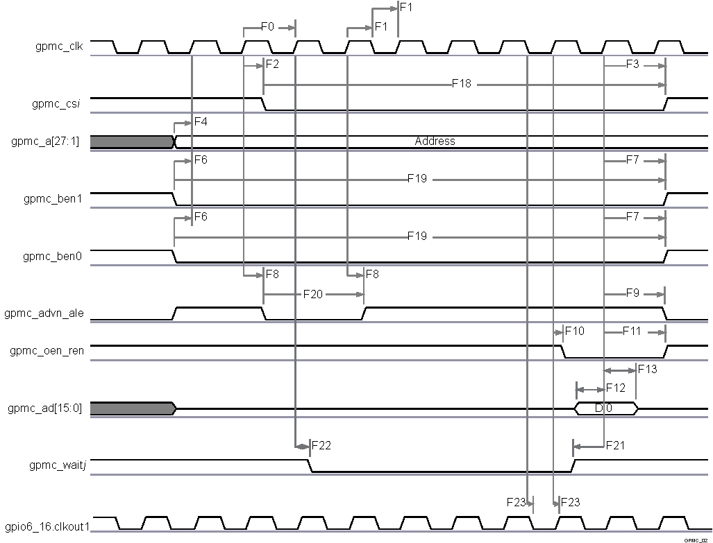 Figure 5-29 GPMC / Nonmultiplexed 16bits NOR Flash - Synchronous Single Read -
(GpmcFCLKDivider = 0)(1)(2)
- In gpmc_csi, i = 0 to 7.
- In gpmc_waitj, j = 0 to 1.
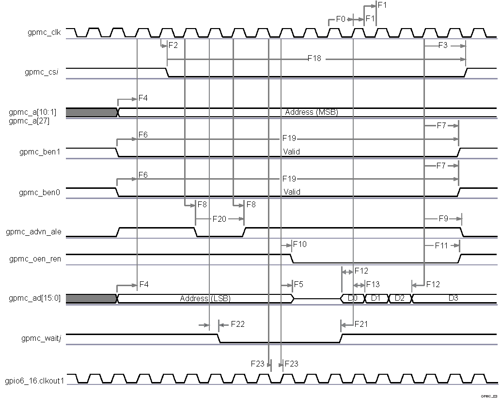 Figure 5-30 GPMC / Multiplexed 16bits NOR Flash - Synchronous Burst Read 4x16 bits -
(GpmcFCLKDivider = 0)(1)(2)
- In gpmc_csi, i= 0 to 7.
- In gpmc_waitj, j = 0 to 1.
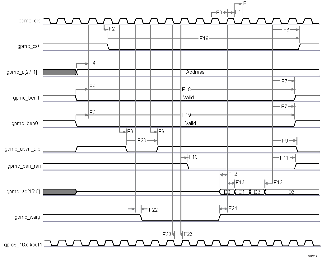 Figure 5-31 GPMC / Nonmultiplexed 16bits NOR Flash - Synchronous Burst Read 4x16 bits -
(GpmcFCLKDivider = 0)(1)(2)
- In gpmc_csi, i = 0 to 7.
- In gpmc_waitj, j = 0 to 1.
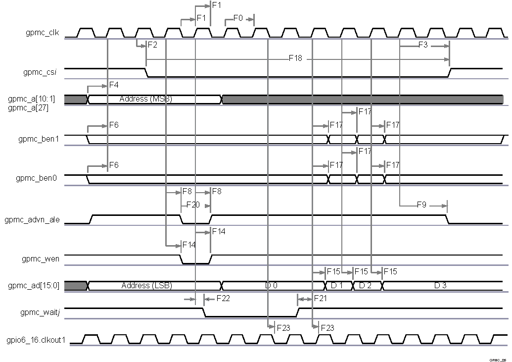 Figure 5-32 GPMC / Multiplexed 16bits NOR Flash - Synchronous Burst Write 4x16bits -
(GpmcFCLKDivider = 0)(1)(2)
- In gpmc_csi, i = 0 to 7.
- In gpmc_waitj, j = 0 to 1.
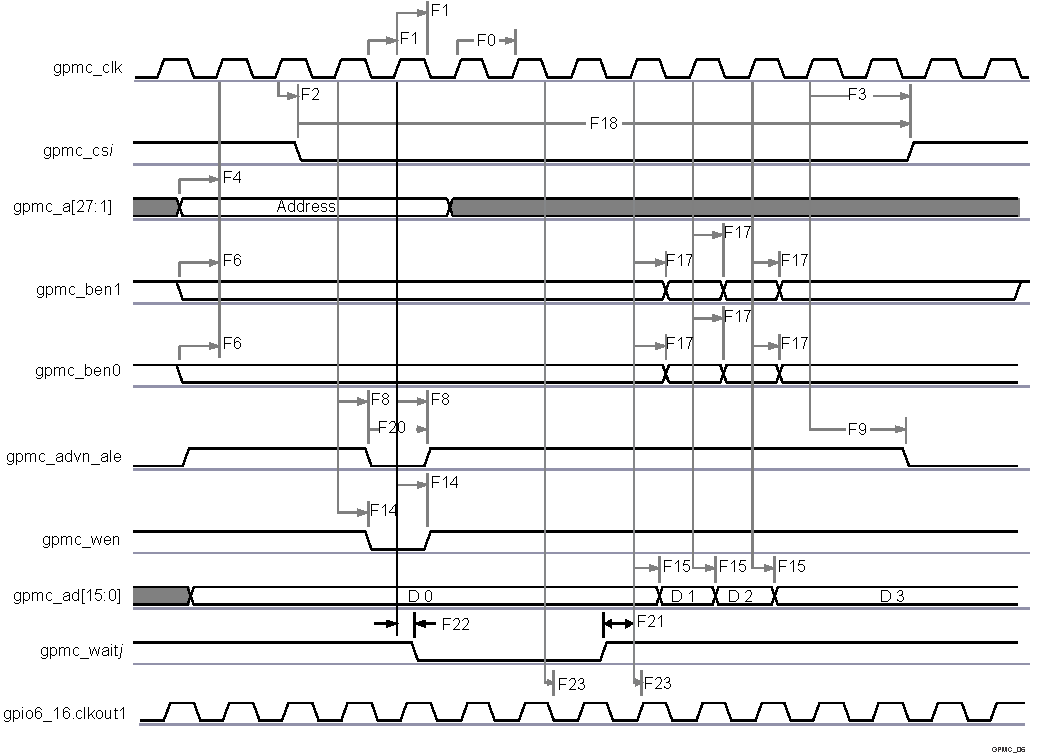 Figure 5-33 GPMC / Nonmultiplexed 16bits NOR Flash - Synchronous Burst Write 4x16bits - (GpmcFCLKDivider = 0)(1)(2)
 - In gpmc_csi, i = 1 to 7.
- In gpmc_waitj, j = 0 to 1.