ZHCSJ46F December 2016 – December 2018 DRA74P , DRA75P
ADVANCE INFORMATION for pre-production products; subject to change without notice.
- 1器件概述
- 2修订历史记录
- 3Device Comparison
-
4Terminal Configuration and Functions
- 4.1 Pin Diagram
- 4.2 Pin Attributes
- 4.3
Signal Descriptions
- 4.3.1 VIP
- 4.3.2 DSS
- 4.3.3 HDMI
- 4.3.4 EMIF
- 4.3.5 GPMC
- 4.3.6 Timers
- 4.3.7 I2C
- 4.3.8 HDQ1W
- 4.3.9 UART
- 4.3.10 McSPI
- 4.3.11 QSPI
- 4.3.12 McASP
- 4.3.13 USB
- 4.3.14 SATA
- 4.3.15 PCIe
- 4.3.16 DCAN and MCAN
- 4.3.17 GMAC_SW
- 4.3.18 MLB
- 4.3.19 eMMC/SD/SDIO
- 4.3.20 GPIO
- 4.3.21 KBD
- 4.3.22 PWM
- 4.3.23 ATL
- 4.3.24 Test Interfaces
- 4.3.25 System and Miscellaneous
- 4.4 Pin Multiplexing
- 4.5 Connections for Unused Pins
-
5Specifications
- 5.1 Absolute Maximum Ratings
- 5.2 ESD Ratings
- 5.3 Power-On Hours (POH)
- 5.4 Recommended Operating Conditions
- 5.5 Operating Performance Points
- 5.6 Power Consumption Summary
- 5.7
Electrical Characteristics
- Table 5-6 LVCMOS DDR DC Electrical Characteristics
- Table 5-7 Dual Voltage LVCMOS I2C DC Electrical Characteristics
- Table 5-8 IQ1833 Buffers DC Electrical Characteristics
- Table 5-9 IHHV1833 Buffers DC Electrical Characteristics
- Table 5-10 LVCMOS OSC Buffers DC Electrical Characteristics
- Table 5-11 BMLB18 Buffers DC Electrical Characteristics
- Table 5-12 BC1833IHHV Buffers DC Electrical Characteristics
- Table 5-13 Dual Voltage SDIO1833 DC Electrical Characteristics
- Table 5-14 Dual Voltage LVCMOS DC Electrical Characteristics
- 5.7.1 HDMIPHY DC Electrical Characteristics
- 5.7.2 USBPHY DC Electrical Characteristics
- 5.7.3 SATAPHY DC Electrical Characteristics
- 5.7.4 PCIEPHY DC Electrical Characteristics
- 5.8 VPP Specifications for One-Time Programmable (OTP) eFuses
- 5.9 Thermal Resistance Characteristics
- 5.10
Timing Requirements and Switching Characteristics
- 5.10.1 Timing Parameters and Information
- 5.10.2 Interface Clock Specifications
- 5.10.3 Power Supply Sequences
- 5.10.4 Clock Specifications
- 5.10.5 Recommended Clock and Control Signal Transition Behavior
- 5.10.6
Peripherals
- 5.10.6.1 Timing Test Conditions
- 5.10.6.2 Virtual and Manual I/O Timing Modes
- 5.10.6.3 VIP
- 5.10.6.4 DSS
- 5.10.6.5 HDMI
- 5.10.6.6 EMIF
- 5.10.6.7 GPMC
- 5.10.6.8 Timers
- 5.10.6.9 I2C
- 5.10.6.10 HDQ1W
- 5.10.6.11 UART
- 5.10.6.12 McSPI
- 5.10.6.13 QSPI
- 5.10.6.14
McASP
- Table 5-79 Timing Requirements for McASP1
- Table 5-80 Timing Requirements for McASP2
- Table 5-81 Timing Requirements for McASP3/4/5/6/7/8
- Table 5-82 Switching Characteristics Over Recommended Operating Conditions for McASP1
- Table 5-83 Switching Characteristics Over Recommended Operating Conditions for McASP2
- Table 5-84 Switching Characteristics Over Recommended Operating Conditions for McASP3/4/5/6/7/8
- 5.10.6.15 USB
- 5.10.6.16 SATA
- 5.10.6.17 PCIe
- 5.10.6.18 CAN
- 5.10.6.19
GMAC_SW
- 5.10.6.19.1
GMAC MII Timings
- Table 5-101 Timing Requirements for miin_rxclk - MII Operation
- Table 5-102 Timing Requirements for miin_txclk - MII Operation
- Table 5-103 Timing Requirements for GMAC MIIn Receive 10/100 Mbit/s
- Table 5-104 Switching Characteristics Over Recommended Operating Conditions for GMAC MIIn Transmit 10/100 Mbits/s
- 5.10.6.19.2 GMAC MDIO Interface Timings
- 5.10.6.19.3
GMAC RMII Timings
- Table 5-109 Timing Requirements for GMAC REF_CLK - RMII Operation
- Table 5-110 Timing Requirements for GMAC RMIIn Receive
- Table 5-111 Switching Characteristics Over Recommended Operating Conditions for GMAC REF_CLK - RMII Operation
- Table 5-112 Switching Characteristics Over Recommended Operating Conditions for GMAC RMIIn Transmit 10/100 Mbits/s
- 5.10.6.19.4
GMAC RGMII Timings
- Table 5-116 Timing Requirements for rgmiin_rxc - RGMIIn Operation
- Table 5-117 Timing Requirements for GMAC RGMIIn Input Receive for 10/100/1000 Mbps
- Table 5-118 Switching Characteristics Over Recommended Operating Conditions for rgmiin_txctl - RGMIIn Operation for 10/100/1000 Mbit/s
- Table 5-119 Switching Characteristics for GMAC RGMIIn Output Transmit for 10/100/1000 Mbps
- 5.10.6.19.1
GMAC MII Timings
- 5.10.6.20 MLB
- 5.10.6.21
eMMC/SD/SDIO
- 5.10.6.21.1
MMC1—SD Card Interface
- 5.10.6.21.1.1 Default speed, 4-bit data, SDR, half-cycle
- 5.10.6.21.1.2 High speed, 4-bit data, SDR, half-cycle
- 5.10.6.21.1.3 SDR12, 4-bit data, half-cycle
- 5.10.6.21.1.4 SDR25, 4-bit data, half-cycle
- 5.10.6.21.1.5 UHS-I SDR50, 4-bit data, half-cycle
- 5.10.6.21.1.6 UHS-I SDR104, 4-bit data, half-cycle
- 5.10.6.21.1.7 UHS-I DDR50, 4-bit data
- 5.10.6.21.2 MMC2 — eMMC
- 5.10.6.21.3 MMC3 and MMC4—SDIO/SD
- 5.10.6.21.1
MMC1—SD Card Interface
- 5.10.6.22 GPIO
- 5.10.6.23 ATL
- 5.10.6.24 System and Miscellaneous Interfaces
- 5.10.7
Emulation and Debug Subsystem
- 5.10.7.1
JTAG
- 5.10.7.1.1
JTAG Electrical Data/Timing
- Table 5-176 Timing Requirements for IEEE 1149.1 JTAG
- Table 5-177 Switching Characteristics Over Recommended Operating Conditions for IEEE 1149.1 JTAG
- Table 5-178 Timing Requirements for IEEE 1149.1 JTAG With RTCK
- Table 5-179 Switching Characteristics Over Recommended Operating Conditions for IEEE 1149.1 JTAG With RTCK
- 5.10.7.1.1
JTAG Electrical Data/Timing
- 5.10.7.2 TPIU
- 5.10.7.1
JTAG
-
6Detailed Description
- 6.1 Description
- 6.2 Functional Block Diagram
- 6.3 MPU
- 6.4 DSP Subsystem
- 6.5 ISS
- 6.6 IVA
- 6.7 EVE
- 6.8 IPU
- 6.9 VPE
- 6.10 GPU
- 6.11 ATL Overview
- 6.12 Memory Subsystem
- 6.13 Interprocessor Communication
- 6.14 Interrupt Controller
- 6.15 EDMA
- 6.16 Peripherals
- 6.17 On-Chip Debug
-
7Applications, Implementation, and Layout
- 7.1 Introduction
- 7.2 Power Optimizations
- 7.3 Core Power Domains
- 7.4 Single-Ended Interfaces
- 7.5
Differential Interfaces
- 7.5.1 General Routing Guidelines
- 7.5.2
USB 2.0 Board Design and Layout Guidelines
- 7.5.2.1 Background
- 7.5.2.2
USB PHY Layout Guide
- 7.5.2.2.1 General Routing and Placement
- 7.5.2.2.2
Specific Guidelines for USB PHY Layout
- 7.5.2.2.2.1 Analog, PLL, and Digital Power Supply Filtering
- 7.5.2.2.2.2 Analog, Digital, and PLL Partitioning
- 7.5.2.2.2.3 Board Stackup
- 7.5.2.2.2.4 Cable Connector Socket
- 7.5.2.2.2.5 Clock Routings
- 7.5.2.2.2.6 Crystals/Oscillator
- 7.5.2.2.2.7 DP/DM Trace
- 7.5.2.2.2.8 DP/DM Vias
- 7.5.2.2.2.9 Image Planes
- 7.5.2.2.2.10 JTAG Interface
- 7.5.2.2.2.11 Power Regulators
- 7.5.2.3 Electrostatic Discharge (ESD)
- 7.5.2.4 References
- 7.5.3 USB 3.0 Board Design and Layout Guidelines
- 7.5.4 HDMI Board Design and Layout Guidelines
- 7.5.5 SATA Board Design and Layout Guidelines
- 7.5.6 PCIe Board Design and Layout Guidelines
- 7.6 Clock Routing Guidelines
- 7.7
DDR2/DDR3 Board Design and Layout Guidelines
- 7.7.1 DDR2/DDR3 General Board Layout Guidelines
- 7.7.2 DDR2 Board Design and Layout Guidelines
- 7.7.3
DDR3 Board Design and Layout Guidelines
- 7.7.3.1 Board Designs
- 7.7.3.2 DDR3 EMIF
- 7.7.3.3 DDR3 Device Combinations
- 7.7.3.4 DDR3 Interface Schematic
- 7.7.3.5 Compatible JEDEC DDR3 Devices
- 7.7.3.6 PCB Stackup
- 7.7.3.7 Placement
- 7.7.3.8 DDR3 Keepout Region
- 7.7.3.9 Bulk Bypass Capacitors
- 7.7.3.10 High-Speed Bypass Capacitors
- 7.7.3.11 Net Classes
- 7.7.3.12 DDR3 Signal Termination
- 7.7.3.13 VREF_DDR Routing
- 7.7.3.14 VTT
- 7.7.3.15 CK and ADDR_CTRL Topologies and Routing Definition
- 7.7.3.16 Data Topologies and Routing Definition
- 7.7.3.17 Routing Specification
- 8Device and Documentation Support
- 9Mechanical Packaging and Orderable Information
7.2.1 Step 1: PCB Stack-up
The PCB stack-up (layer assignment) is an important factor in determining the optimal performance of the power distribution system. An optimized PCB stack-up for higher power integrity performance can be achieved by following these recommendations:
- Power and ground plane pairs must be closely coupled together. The capacitance formed between the planes can decouple the power supply at high frequencies. Whenever possible, the power and ground planes must be solid to provide continuous return path for return current.
- Use a thin dielectric between the power and ground plane pair. Capacitance is inversely proportional to the separation of the plane pair. Minimizing the separation distance (the dielectric thickness) maximizes the capacitance.
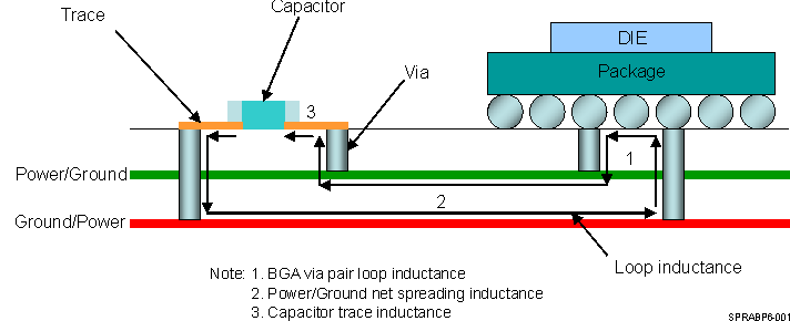
- Optimize the power and ground plane pair carrying high current supplies to key component power domains as close as possible to the same surface where these components are placed (see Figure 7-1). This will help to minimize “loop inductance” encountered between supply decoupling capacitors and component supply inputs and between power and ground plane pairs.
NOTE
1-2oz Cu weight for power / ground plane is preferred to enable better PCB heat spreading, helping to reduce Processor junction temperatures. In addition, it is preferable to have the power / ground planes be adjacent to the PCB surface on which the Processor is mounted.
 Figure 7-1 Minimize Loop Inductance With Proper Layer Assignment
 The placement of power and ground planes in the PCB stackup (determined by layer assignment) has a significant impact on the parasitic inductances of power current path as shown in Figure 7-1. For this reason, it is recommended to consider layer order in the early stages of the PCB PDN design cycle, putting high-priority supplies in the top half of the stackup (assuming high load and priority components are mounted on the top-side of PCB) and low-priority supplies in the bottom half of the stackup as shown in the examples below (vias have parasitic inductances which impact the bottom layers more, so it is advised to put the sensitive and high-priority power supplies on the top/same layers).
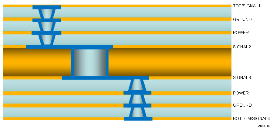
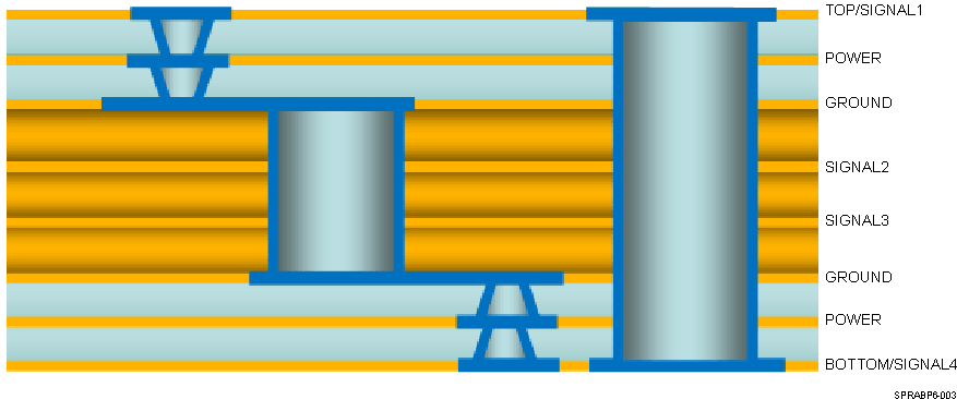
Two PCB stack-ups with layer assignments and via types that can enable an optimize PDN are shown in Figure 7-2 and Figure 7-3.
 Figure 7-2 Layer PCB With High Density Interconnect (HDI) Vias
  Figure 7-3 Layer PCB With Plated Through Holes (PTH) Vias