ZHCSI52G August 2016 – March 2019 DRA780 , DRA781 , DRA782 , DRA783 , DRA785 , DRA786 , DRA787 , DRA788
PRODUCTION DATA.
- 1器件概述
- 2修订历史记录
- 3Device Comparison
-
4Terminal Configuration and Functions
- 4.1 Pin Diagram
- 4.2 Pin Attributes
- 4.3
Signal Descriptions
- 4.3.1 VIP
- 4.3.2 DSS
- 4.3.3 SD_DAC
- 4.3.4 ADC
- 4.3.5 Camera Control
- 4.3.6 CPI
- 4.3.7 CSI2
- 4.3.8 EMIF
- 4.3.9 GPMC
- 4.3.10 Timers
- 4.3.11 I2C
- 4.3.12 UART
- 4.3.13 McSPI
- 4.3.14 QSPI
- 4.3.15 McASP
- 4.3.16 DCAN and MCAN
- 4.3.17 GMAC_SW
- 4.3.18 SDIO Controller
- 4.3.19 GPIO
- 4.3.20 ePWM
- 4.3.21 ATL
- 4.3.22 Test Interfaces
- 4.3.23 System and Miscellaneous
- 4.3.24 Power Supplies
- 4.4 Pin Multiplexing
- 4.5 Connections for Unused Pins
-
5Specifications
- 5.1 Absolute Maximum Ratings
- 5.2 ESD Ratings
- 5.3 Power on Hour (POH) Limits
- 5.4 Recommended Operating Conditions
- 5.5 Operating Performance Points
- 5.6 Power Consumption Summary
- 5.7
Electrical Characteristics
- Table 5-6 LVCMOS DDR DC Electrical Characteristics
- Table 5-7 Dual Voltage LVCMOS I2C DC Electrical Characteristics
- Table 5-8 IQ1833 Buffers DC Electrical Characteristics
- Table 5-9 IHHV1833 Buffers DC Electrical Characteristics
- Table 5-10 LVCMOS Analog OSC Buffers DC Electrical Characteristics
- Table 5-11 Dual Voltage LVCMOS DC Electrical Characteristics
- Table 5-12 Analog-to-Digital ADC Subsystem Electrical Specifications
- 5.8 Thermal Characteristics
- 5.9
Timing Requirements and Switching Characteristics
- 5.9.1 Timing Parameters and Information
- 5.9.2 Interface Clock Specifications
- 5.9.3 Power Supply Sequences
- 5.9.4 Clock Specifications
- 5.9.5 Recommended Clock and Control Signal Transition Behavior
- 5.9.6
Peripherals
- 5.9.6.1 Timing Test Conditions
- 5.9.6.2 VIP
- 5.9.6.3 DSS
- 5.9.6.4 EMIF
- 5.9.6.5 GPMC
- 5.9.6.6 GP Timers
- 5.9.6.7 I2C
- 5.9.6.8 UART
- 5.9.6.9 McSPI
- 5.9.6.10 QSPI
- 5.9.6.11
McASP
- Table 5-50 Timing Requirements for McASP1
- Table 5-51 Timing Requirements for McASP2
- Table 5-52 Timing Requirements for McASP3
- Table 5-53 Switching Characteristics Over Recommended Operating Conditions for McASP1
- Table 5-54 Switching Characteristics Over Recommended Operating Conditions for McASP2
- Table 5-55 Switching Characteristics Over Recommended Operating Conditions for McASP3
- 5.9.6.12 DCAN and MCAN
- 5.9.6.13
GMAC_SW
- 5.9.6.13.1 GMAC MDIO Interface Timings
- 5.9.6.13.2
GMAC RGMII Timings
- Table 5-63 Timing Requirements for rgmiin_rxc - RGMIIn Operation
- Table 5-64 Timing Requirements for GMAC RGMIIn Input Receive for 10/100/1000 Mbps
- Table 5-65 Switching Characteristics Over Recommended Operating Conditions for rgmiin_txctl - RGMIIn Operation for 10/100/1000 Mbit/s
- Table 5-66 Switching Characteristics for GMAC RGMIIn Output Transmit for 10/100/1000 Mbps
- 5.9.6.14 SDIO Controller
- 5.9.6.15 GPIO
- 5.9.6.16 ATL
- 5.9.7
Emulation and Debug Subsystem
- 5.9.7.1
JTAG Electrical Data/Timing
- Table 5-78 Timing Requirements for IEEE 1149.1 JTAG
- Table 5-79 Switching Characteristics Over Recommended Operating Conditions for IEEE 1149.1 JTAG
- Table 5-80 Timing Requirements for IEEE 1149.1 JTAG With RTCK
- Table 5-81 Switching Characteristics Over Recommended Operating Conditions for IEEE 1149.1 JTAG With RTCK
- 5.9.7.2 Trace Port Interface Unit (TPIU)
- 5.9.7.1
JTAG Electrical Data/Timing
-
6Detailed Description
- 6.1 Description
- 6.2 Functional Block Diagram
- 6.3 DSP Subsystem
- 6.4 IPU
- 6.5 EVE
- 6.6 Memory Subsystem
- 6.7 Interprocessor Communication
- 6.8 Interrupt Controller
- 6.9 EDMA
- 6.10 Peripherals
- 6.11 On-Chip Debug
-
7Applications, Implementation, and Layout
- 7.1 Introduction
- 7.2 Power Optimizations
- 7.3 Core Power Domains
- 7.4 Single-Ended Interfaces
- 7.5 Differential Interfaces
- 7.6 Clock Routing Guidelines
- 7.7 DDR2 Board Design and Layout Guidelines
- 7.8
DDR3 Board Design and Layout Guidelines
- 7.8.1 DDR3 General Board Layout Guidelines
- 7.8.2
DDR3 Board Design and Layout Guidelines
- 7.8.2.1 Board Designs
- 7.8.2.2 DDR3 Device Combinations
- 7.8.2.3 DDR3 Interface Schematic
- 7.8.2.4 Compatible JEDEC DDR3 Devices
- 7.8.2.5 PCB Stackup
- 7.8.2.6 Placement
- 7.8.2.7 DDR3 Keepout Region
- 7.8.2.8 Bulk Bypass Capacitors
- 7.8.2.9 High-Speed Bypass Capacitors
- 7.8.2.10 Net Classes
- 7.8.2.11 DDR3 Signal Termination
- 7.8.2.12 VTT
- 7.8.2.13 CK and ADDR_CTRL Topologies and Routing Definition
- 7.8.2.14 Data Topologies and Routing Definition
- 7.8.2.15 Routing Specification
- 7.9 CVIDEO/SD-DAC Guidelines and Electrical Data/Timing
- 8Device and Documentation Support
- 9Mechanical, Packaging, and Orderable Information
5.9.6.5.3 GPMC/NAND Flash Interface Asynchronous Timing
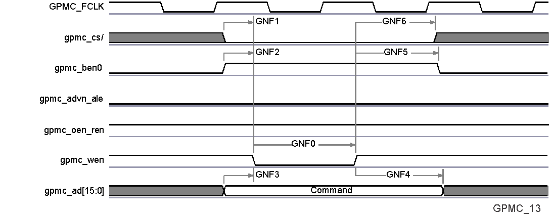
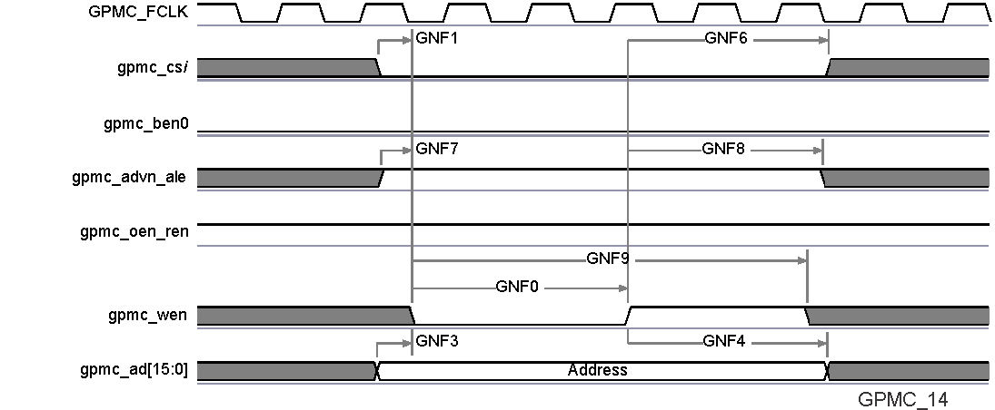
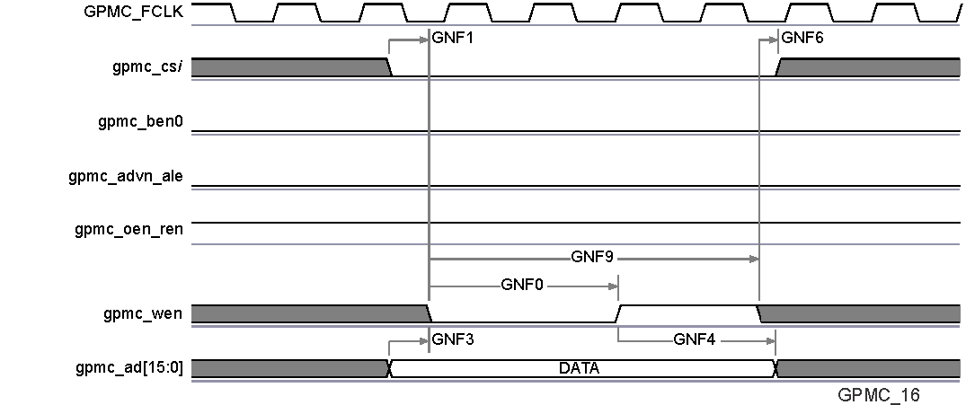
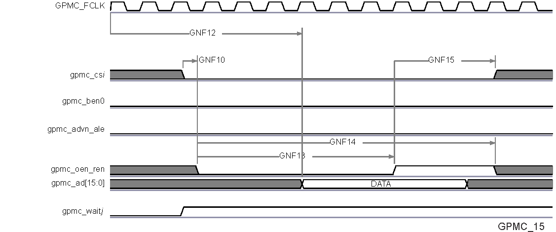
Table 5-37 and Table 5-38 assume testing over the recommended operating conditions and electrical characteristic conditions below (see Figure 5-34, Figure 5-35, Figure 5-36 and Figure 5-37).
Table 5-37 GPMC/NAND Flash Interface Timing Requirements(1)
| NO. | PARAMETER | DESCRIPTION | MIN | MAX | UNIT | |
|---|---|---|---|---|---|---|
| GNF12 | tacc(DAT) | Data maximum access time (GPMC_FCLK Cycles) | J | cycles | ||
| - | tsu(DV-OEH) | Setup time, read gpmc_ad[15:0] valid before gpmc_oen_ren high | 1.9 | ns | ||
| - | - | th(OEH-DV) | Hold time, read gpmc_ad[15:0] valid after gpmc_oen_ren high | 1 | ns |
- J = AccessTime × (TimeParaGranularity + 1)
Table 5-38 GPMC/NAND Flash Interface Switching Characteristics
| NO. | PARAMETER | DESCRIPTION | MIN | MAX | UNIT | |
|---|---|---|---|---|---|---|
| - | tr(DO) | Rising time, gpmc_ad[15:0] output data | 0.447 | 4.067 | ns | |
| - | - | tf(DO) | Fallling time, gpmc_ad[15:0] output data | 0.43 | 4.463 | ns |
| GNF0 | tw(nWEV) | Pulse duration, gpmc_wen valid time | A (1) | ns | ||
| GNF1 | td(nCSV-nWEV) | Delay time, gpmc_cs[7:0] valid to gpmc_wen valid | B - 0.2 (2) | B + 2.0 (2) | ns | |
| GNF2 | td(CLEH-nWEV) | Delay time, gpmc_ben[1:0] high to gpmc_wen valid | C - 0.2 (3) | C + 2.0 (3) | ns | |
| GNF3 | td(nWEV-DV) | Delay time, gpmc_ad[15:0] valid to gpmc_wen valid | D - 0.2 (4) | D + 2.0 (4) | ns | |
| GNF4 | td(nWEIV-DIV) | Delay time, gpmc_wen invalid to gpmc_ad[15:0] invalid | E - 0.2 (5) | E + 2.0 (5) | ns | |
| GNF5 | td(nWEIV-CLEIV) | Delay time, gpmc_wen invalid to gpmc_ben[1:0] invalid | F - 0.2 (6) | F + 2.0 (6) | ns | |
| GNF6 | td(nWEIV-nCSIV) | Delay time, gpmc_wen invalid to gpmc_cs[7:0] invalid | G - 0.2 (7) | G + 2.0 (7) | ns | |
| GNF7 | td(ALEH-nWEV) | Delay time, gpmc_advn_ale high to gpmc_wen valid | C - 0.2 (3) | C + 2.0 (3) | ns | |
| GNF8 | td(nWEIV-ALEIV) | Delay time, gpmc_wen invalid to gpmc_advn_ale invalid | F - 0.2 (6) | F + 2.0 (6) | ns | |
| GNF9 | tc(nWE) | Cycle time, write cycle time | H (8) | ns | ||
| GNF10 | td(nCSV-nOEV) | Delay time, gpmc_cs[7:0] valid to gpmc_oen_ren valid | I - 0.2 (9) | I + 2.0 (9) | ns | |
| GNF13 | tw(nOEV) | Pulse duration, gpmc_oen_ren valid time | K | ns | ||
| GNF14 | tc(nOE) | Cycle time, read cycle time | L (10) | ns | ||
| GNF15 | td(nOEIV-nCSIV) | Delay time, gpmc_oen_ren invalid to gpmc_cs[7:0] invalid | M - 0.2 (11) | M + 2.0 (11) | ns |
- A = (WEOffTime – WEOnTime) × (TimeParaGranularity + 1) × GPMC_FCLK
- B = ((WEOnTime – CSOnTime) × (TimeParaGranularity + 1) + 0.5 × (WEExtraDelay – CSExtraDelay)) × GPMC_FCLK
- C = ((WEOnTime – ADVOnTime) × (TimeParaGranularity + 1) + 0.5 × (WEExtraDelay – ADVExtraDelay)) × GPMC_FCLK
- D = (WEOnTime × (TimeParaGranularity + 1) + 0.5 × WEExtraDelay ) × GPMC_FCLK
- E = (WrCycleTime – WEOffTime × (TimeParaGranularity + 1) – 0.5 × WEExtraDelay ) × GPMC_FCLK
- F = (ADVWrOffTime – WEOffTime × (TimeParaGranularity + 1) + 0.5 × (ADVExtraDelay – WEExtraDelay ) × GPMC_FCLK
- G = (CSWrOffTime – WEOffTime × (TimeParaGranularity + 1) + 0.5 × (CSExtraDelay – WEExtraDelay ) × GPMC_FCLK
- H = WrCycleTime × (1 + TimeParaGranularity) × GPMC_FCLK
- I = ((OEOffTime + (n – 1) × PageBurstAccessTime – CSOnTime) × (TimeParaGranularity + 1) + 0.5 × (OEExtraDelay – CSExtraDelay)) × GPMC_FCLK
- K = (OEOffTime – OEOnTime) × (1 + TimeParaGranularity) × GPMC_FCLK
- L = RdCycleTime × (1 + TimeParaGranularity) × GPMC_FCLK
- M = (CSRdOffTime – OEOffTime × (TimeParaGranularity + 1) + 0.5 × (CSExtraDelay – OEExtraDelay ) × GPMC_FCLK
 Figure 5-34 GPMC / NAND Flash - Command Latch Cycle Timing(1)
 - In gpmc_csi, i = 0 to 7.
 Figure 5-35 GPMC / NAND Flash - Address Latch Cycle Timing(1)
 - In gpmc_csi, i = 0 to 7.
- GNF12 parameter illustrates amount of time required to internally sample input Data. It is expressed in number of GPMC functional clock cycles. From start of read cycle and after GNF12 functional clock cycles, input data will be internally sampled by active functional clock edge. GNF12 value must be stored inside AccessTime register bits field.
- GPMC_FCLK is an internal clock (GPMC functional clock) not provided externally.
- In gpmc_csi, i = 0 to 7. In gpmc_waitj, j = 0 to 1.
 Figure 5-37 GPMC / NAND Flash - Data Write Cycle Timing(1)
 - In gpmc_csi, i = 0 to 7.
NOTE
To configure the desired virtual mode the user must set MODESELECT bit and DELAYMODE bitfield for each corresponding pad control register.
The pad control registers are presented Table 4-29 and described in Device TRM, Control Module section.
