SPRS975H August 2016 – February 2020 DRA780 , DRA781 , DRA782 , DRA783 , DRA785 , DRA786 , DRA787 , DRA788
PRODUCTION DATA.
- 1Device Overview
- 2Revision History
- 3Device Comparison
-
4Terminal Configuration and Functions
- 4.1 Pin Diagram
- 4.2 Pin Attributes
- 4.3
Signal Descriptions
- 4.3.1 VIP
- 4.3.2 DSS
- 4.3.3 SD_DAC
- 4.3.4 ADC
- 4.3.5 Camera Control
- 4.3.6 CPI
- 4.3.7 CSI2
- 4.3.8 EMIF
- 4.3.9 GPMC
- 4.3.10 Timers
- 4.3.11 I2C
- 4.3.12 UART
- 4.3.13 McSPI
- 4.3.14 QSPI
- 4.3.15 McASP
- 4.3.16 DCAN and MCAN
- 4.3.17 GMAC_SW
- 4.3.18 SDIO Controller
- 4.3.19 GPIO
- 4.3.20 PWMSS
- 4.3.21 ATL
- 4.3.22 Test Interfaces
- 4.3.23 System and Miscellaneous
- 4.3.24 Power Supplies
- 4.4 Pin Multiplexing
- 4.5 Connections for Unused Pins
-
5Specifications
- 5.1 Absolute Maximum Ratings
- 5.2 ESD Ratings
- 5.3 Power-On Hours (POH)
- 5.4 Recommended Operating Conditions
- 5.5 Operating Performance Points
- 5.6 Power Consumption Summary
- 5.7
Electrical Characteristics
- Table 5-6 LVCMOS DDR DC Electrical Characteristics
- Table 5-7 Dual Voltage LVCMOS I2C DC Electrical Characteristics
- Table 5-8 IQ1833 Buffers DC Electrical Characteristics
- Table 5-9 IHHV1833 Buffers DC Electrical Characteristics
- Table 5-10 LVCMOS Analog OSC Buffers DC Electrical Characteristics
- Table 5-11 Dual Voltage LVCMOS DC Electrical Characteristics
- Table 5-12 Analog-to-Digital ADC Subsystem Electrical Specifications
- 5.8 Thermal Characteristics
- 5.9
Timing Requirements and Switching Characteristics
- 5.9.1 Timing Parameters and Information
- 5.9.2 Interface Clock Specifications
- 5.9.3 Power Supply Sequences
- 5.9.4 Clock Specifications
- 5.9.5 Recommended Clock and Control Signal Transition Behavior
- 5.9.6
Peripherals
- 5.9.6.1 Timing Test Conditions
- 5.9.6.2 VIP
- 5.9.6.3 DSS
- 5.9.6.4 EMIF
- 5.9.6.5 GPMC
- 5.9.6.6 GP Timers
- 5.9.6.7 I2C
- 5.9.6.8 UART
- 5.9.6.9 McSPI
- 5.9.6.10 QSPI
- 5.9.6.11
McASP
- Table 5-50 Timing Requirements for McASP1
- Table 5-51 Timing Requirements for McASP2
- Table 5-52 Timing Requirements for McASP3
- Table 5-53 Switching Characteristics Over Recommended Operating Conditions for McASP1
- Table 5-54 Switching Characteristics Over Recommended Operating Conditions for McASP2
- Table 5-55 Switching Characteristics Over Recommended Operating Conditions for McASP3
- 5.9.6.12 DCAN and MCAN
- 5.9.6.13
GMAC_SW
- 5.9.6.13.1 GMAC MDIO Interface Timings
- 5.9.6.13.2
GMAC RGMII Timings
- Table 5-63 Timing Requirements for rgmiin_rxc - RGMIIn Operation
- Table 5-64 Timing Requirements for GMAC RGMIIn Input Receive for 10/100/1000 Mbps
- Table 5-65 Switching Characteristics Over Recommended Operating Conditions for rgmiin_txctl - RGMIIn Operation for 10/100/1000 Mbit/s
- Table 5-66 Switching Characteristics for GMAC RGMIIn Output Transmit for 10/100/1000 Mbps
- 5.9.6.14 SDIO Controller
- 5.9.6.15 GPIO
- 5.9.6.16 ATL
- 5.9.7
Emulation and Debug Subsystem
- 5.9.7.1
JTAG Electrical Data/Timing
- Table 5-78 Timing Requirements for IEEE 1149.1 JTAG
- Table 5-79 Switching Characteristics Over Recommended Operating Conditions for IEEE 1149.1 JTAG
- Table 5-80 Timing Requirements for IEEE 1149.1 JTAG With RTCK
- Table 5-81 Switching Characteristics Over Recommended Operating Conditions for IEEE 1149.1 JTAG With RTCK
- 5.9.7.2 Trace Port Interface Unit (TPIU)
- 5.9.7.1
JTAG Electrical Data/Timing
-
6Detailed Description
- 6.1 Overview
- 6.2 Processor Subsystems
- 6.3 Accelerators and Coprocessors
- 6.4
Other Subsystems
- 6.4.1 Memory Subsystem
- 6.4.2 Interprocessor Communication
- 6.4.3 Interrupt Controller
- 6.4.4 EDMA
- 6.4.5 Peripherals
- 6.4.6 On-Chip Debug
-
7Applications, Implementation, and Layout
- 7.1 Introduction
- 7.2 Power Optimizations
- 7.3 Core Power Domains
- 7.4 Single-Ended Interfaces
- 7.5 Differential Interfaces
- 7.6 Clock Routing Guidelines
- 7.7 DDR2 Board Design and Layout Guidelines
- 7.8
DDR3 Board Design and Layout Guidelines
- 7.8.1 DDR3 General Board Layout Guidelines
- 7.8.2
DDR3 Board Design and Layout Guidelines
- 7.8.2.1 Board Designs
- 7.8.2.2 DDR3 Device Combinations
- 7.8.2.3 DDR3 Interface Schematic
- 7.8.2.4 Compatible JEDEC DDR3 Devices
- 7.8.2.5 PCB Stackup
- 7.8.2.6 Placement
- 7.8.2.7 DDR3 Keepout Region
- 7.8.2.8 Bulk Bypass Capacitors
- 7.8.2.9 High Speed Bypass Capacitors
- 7.8.2.10 Net Classes
- 7.8.2.11 DDR3 Signal Termination
- 7.8.2.12 VTT
- 7.8.2.13 CK and ADDR_CTRL Topologies and Routing Definition
- 7.8.2.14 Data Topologies and Routing Definition
- 7.8.2.15 Routing Specification
- 7.9 CVIDEO/SD-DAC Guidelines and Electrical Data/Timing
- 8Device and Documentation Support
- 9Mechanical, Packaging, and Orderable Information
5.9.3 Power Supply Sequences
This section describes the power-up and power-down sequence required to ensure proper device operation.
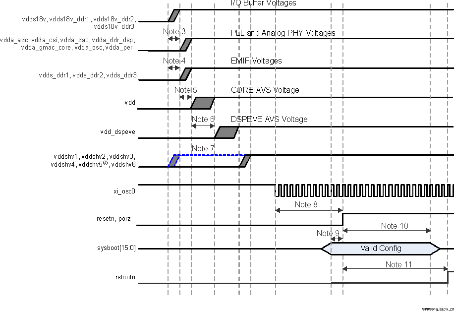
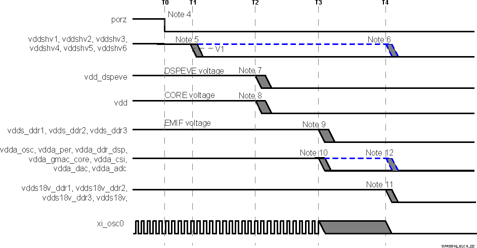
Figure 5-4 through Figure 5-8, and associated notes describes the device Recommended Power Sequencing.
 Figure 5-4 Power-Up Sequencing
 - Grey shaded areas are windows where it is valid to ramp-up a voltage rail.
- Blue dashed lines are not valid windows but show alternate ramp-up possibilities based on whether I/O voltage levels are 1.8V or 3.3V (see associated note for more details).
- vdds18v_* and vdda_* rails should not be combined for best performance to avoid transient switching noise impacts on analog domains. vdda_* should not ramp-up before vdds18v_* but could ramp concurrently if design ensures final operational voltage will not be reached until after vdds18v. The preferred sequence is to follow all vdds18v_* to ensure circuit components and PCB design do not cause an inadvertent violation.
- vdds_ddr* should not ramp-up before vdds18v_*. The preferred sequence is to follow all vdds18v_* to ensure circuit components and PCB design do not cause an inadvertent violation. vdds_ddr* can ramp-up before, concurrently or after vdda_*, there are no dependencies between vdds_ddr* and vdda_* domains.
- vdds_ddr* supplies can be combined with vdds18v_* and vdds18v_ddr supplies for DDR2 mode of operation (1.8V) and ramped up together for simplified power sequencing.
- If vdds18v_ddr and vdds_ddr* are kept separate from vdds18v_* on board, then this combined DDR supply can come up together or after the vdds18v_* supply. The DDR supply in this case should never ramp up before the vdds18v_*.
- vdd should not ramp-up before vdds18v_* or vdds_ddr* domains.
- vdd_dspeve must not exceed vdd core supply and maintain at least 150mV lower voltage on vdd_dspeve vs vdd. vdd_dspeve could ramp concurrently with vdd if design ensures final operational voltage will not be reached until after vdd and maintains minimum of 150mV less than vdd during entire ramp time. The preferred sequence is to follow vdd to ensure circuit components and PCB design do not cause an inadvertent violation.
- If any of the vddshv[1-6] power rails are used for 1.8V I/O signaling, then these rails can be combined with vdds18v_*.
If 3.3V I/O signaling is required, then these rails must be the last to ramp following vdd_dspeve. - resetn and porz must remain asserted low for a minimum of 12P(12) after xi_osc0 is stable at a valid frequency.
- Setup time: SYSBOOT[15:0] pins must be valid 2P(12) before porz is de-asserted high.
- Hold time: SYSBOOT[15:0] pins must be valid 15P(12) after porz is de-asserted high.
- resetn to rstoutn delay is 2ms.
- P = 1/(SYS_CLK1/610) frequency in ns.
- Ramped Up is defined as reaching the minimum operational voltage level for the corresponding power domain. For information about voltage levels, refer to , Recommended Operating Conditions.
 Figure 5-5 Recommended Power-Down Sequencing
 - T1 ≥ 100 µs; T2 = 500 µs; T3 = 1.0 ms; T4 = 1.5ms; V1 = 2.7 V. All "Tn" markers are intended to show total elapsed time, not interval times.
- Terminology:
- VOPR MIN = Minimum Operational Voltage level that ensures device functionality and specified performance in Section 5.4, Recommended Operating Conditions.
- VOFF = OFF Voltage level is defined to be less than 0.6 V where any current draw has no impact to POH.
- Ramp Down = transition time from VOPR MIN to VOFF and is slew rate independent.
- General timing diagram items:
- Grey shaded areas show valid transition times for supplies between VOPR MIN and VOFF.
- Blue dashed lines are not valid windows but show alternate ramp possibilities based on the associated note.
- Dashed vertical lines show approximate elapse times based upon TI recommended PMIC power-down sequencer circuit performance.
- porz must be asserted low for 100 µs min to ensure SoC is set to a safe functional state before any voltage begins to ramp down.
- vddshv[1-6] domains supplied by 3.3 V:
- must remain greater than 2.7 V to enable Dual Voltage GPIO selector circuit operation for 100 µs min after porz is asserted low.
- must be in first group of supplies ramping down after porz has been asserted low for 100 µs min.
- must not exceed vdds18v by more than 2 V during ramp down, see Figure 5-6, "vdds18v versus vddshv[1-6] Discharge Relationship".
- vddshv[1-6] domains supplied by 1.8 V must ramp down concurrently with vdds18v and be sourced from common vdds18v supply.
- vdd_dspeve domain can ramp down before or concurrently with vdd.
- vdd must ramp down after or concurrently with vdd_dspeve.
- vdds_ddr[1-3] domains:
- should ramp down after vdd begins ramping down.
- If DDR2 memory is used (requiring 1.8V supply),
- then vdds_ddr[1-3] can be combined with vdds18v and vdds18v_ddr[1-3] domains and sourced from a common supply. Accordingly, all domains can ramp down concurrently with vdds18v.
- if vdds_ddr[1-3] and vdds18v_ddr[1-3] are combined but kept separate from vdds18v, then the combined 1.8V DDR supply can ramp down before or concurrently with vdds18v.
- vdda_* domains:
- can ramp down before, concurrently or after vdds_ddr[1-3], there is no dependency between these supplies.
- can ramp down before or concurrently with vdds18v.
- must satisfy the vdds18v versus vdda_* discharge relationship (see Figure 5-8) if any of the vdda_* disable point is later or discharge rate is slower than vdds18v.
- vdds18v domain:
- should maintain VOPR MIN (VNOM -5% = 1.71 V) until all other supplies start to ramp down.
- must satisfy the vdds18v versus vddshv[1-6] discharge relationship (see Figure 5-6) if any of the vddshv[1-6] is operating at 3.3 V.
- must satisfy the vdds18v versus vdds_ddr[1-3] discharge relationship ( see Figure 5-7) if vdds_ddr[1-3] discharge rate is slower than vdds18v.
Figure 5-6 describes vddshv[1-6] supplies falling before vdds18v supplies delta.
![DRA780 DRA781 DRA782 DRA783 DRA784 DRA785 DRA786 DRA787 DRA788 vdds18v versus vddshv[1-6] Discharge Relationship DRA780 DRA781 DRA782 DRA783 DRA784 DRA785 DRA786 DRA787 DRA788 SPRS916_ELCH_03.gif](/ods/images/SPRS975H/SPRS916_ELCH_03.gif) Figure 5-6 vdds18v versus vddshv[1-6] Discharge Relationship
Figure 5-6 vdds18v versus vddshv[1-6] Discharge Relationship - Vdelta MAX = 2V
If vdds18v and vdds_ddr* are disabled at the same time due to a loss of input power event or if vdds_ddr* discharges more slowly than vdds18v, analysis has shown no reliability impacts when the elapsed time period beginning with vdds18v dropping below 1.0 V and ending with vdds_ddr* dropping below 0.6 V is less than 10 ms (Figure 5-7).
 Figure 5-7 vdds18v and vdds_ddr* Discharge Relationship(1)
 - V1 > 1.0 V; V2 < 0.6 V; T1 < 10ms.
 Figure 5-8 vdds18v and vdda_* Discharge Relationship(3)
 - vdda_* can be ≥ vdds18v, until vdds18v drops below 1.62 V.
- vdds18v must be ≥ vdda_*, until vdds18v reaches 0.6 V.
- V1 = 1.62 V; V2 < 0.6 V.
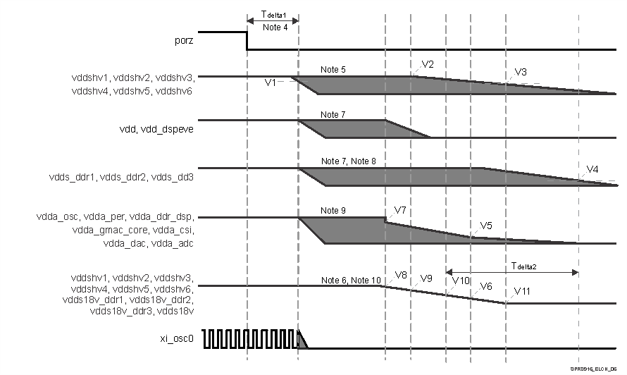
Figure 5-6 through Figure 5-9 and associated notes described the device Abrupt Power Down Sequence.
A ”loss of input power event” occurs when the system’s input power is unexpectedly removed. Normally, the recommended power-down sequence should be followed and can be accomplished within 1.5-2 ms of elapsed time. This is the typical range of elapsed time available following a loss of power event, see Section 7.3.7, Loss of Input Power Event for design recommendations. If sufficient elapse time is not provided, then an “abrupt” power-down sequence can be supported without impacting POH reliability if all of the following conditions are met (Figure 5-9).
 Figure 5-9 Abrupt Power-Down Sequencing(1)
 - V1 = 2.7 V; V2 = 3.3 V; V3 = 2.0 V; V4 = V5 = V6 = 0.6 V; V7 = V8 = 1.62 V; V9 = 1.3 V; V10 = 1.0 V; V11 = 0.0 V; Tdelta1 > 100 µs; Tdelta2 < 10 ms.
- Terminology:
- VOPR MIN = Minimum Operational Voltage level that ensures device functionality and specified performance in Section 5.4, Recommended Operating Conditions.
- VOFF = OFF Voltage level is defined to be less than 0.6 V, where any current draw has no impact to POH.
- Ramp Down = transition time from VOPR MIN to VOFF and is slew rate independent.
- General timing diagram items:
- Grey shaded areas show valid transition times for supplies between VOPR MIN and VOFF.
- Dashed vertical lines show approximate elapse times based upon TI recommended PMIC power-down sequencer circuit performance.
- porz must be asserted low for 100 µs min to ensure SoC is set to a safe functional state before any voltage begins to ramp down.
- vddshv[1-6] domains supplied by 3.3 V:
- must remain greater than 2.7 V to enable Dual Voltage GPIO selector circuit operation for 100µs min, after porz is asserted low.
- must not exceed vdds18v voltage level by more than 2V during ramp down, until vdds18v drops below VOFF (0.6 V).
- vddshv[1-6] domains supplied by 1.8 V must ramp down concurrently with vdds18v and be sourced from common vdds18v supply.
- vdd_dspeve, vdd, vdds_ddr[1-3], vdda_* domains can all start to ramp down in any order after 100 µs low assertion of porz.
- vdds_ddr* domains:
- can remain at VOPR MIN or a level greater than vdds18v during ramp down.
- elapsed time from vdds18v dropping below 1.0 V to vdds_ddr[1-3] dropping below 0.6 V must not exceed 10 ms.
- vdda_* domains:
- can start to ramp down before or concurrently with vdds18v.
- must not exceed vdds18v voltage level after vdds18v drops below 1.62 V until vdds18v drops below VOFF (0.6 V).
- vdds18v domain should maintain a minimum level of 1.62 V (VNOM – 10%) until vdd_dspeve and vdd start to ramp down.