ZHCSKS2E april 2020 – june 2023 DRA821U , DRA821U-Q1
PRODUCTION DATA
- 1
- 1 特性
- 2 应用
- 3 说明
- 4 Revision History
- 5 Device Comparison
-
6 Terminal Configuration and Functions
- 6.1 Pin Diagram
- 6.2 Pin Attributes
- 6.3
Signal Descriptions
- 6.3.1 ADC
- 6.3.2 DDRSS
- 6.3.3 GPIO
- 6.3.4 I2C
- 6.3.5 I3C
- 6.3.6 MCAN
- 6.3.7 MCSPI
- 6.3.8 UART
- 6.3.9 MDIO
- 6.3.10 CPSW2G
- 6.3.11 CPSW5G
- 6.3.12 ECAP
- 6.3.13 EQEP
- 6.3.14 EPWM
- 6.3.15 USB
- 6.3.16 SERDES
- 6.3.17 OSPI
- 6.3.18 Hyperbus
- 6.3.19 GPMC
- 6.3.20 MMC
- 6.3.21 CPTS
- 6.3.22 MCASP
- 6.3.23 DMTIMER
- 6.3.24 Emulation and Debug
- 6.3.25 System and Miscellaneous
- 6.3.26 Power Supply
- 6.4 Pin Multiplexing
- 6.5 Connections for Unused Pins
-
7 Specifications
- 7.1 Absolute Maximum Ratings
- 7.2 ESD Ratings
- 7.3 Recommended Operating Conditions
- 7.4 Power-On-Hours (POH)
- 7.5 Operating Performance Points
- 7.6
Electrical Characteristics
- 7.6.1 I2C, Open-Drain, Fail-Safe (I2C OD FS) Electrical Characteristics
- 7.6.2 Fail-Safe Reset (FS Reset) Electrical Characteristics
- 7.6.3 HFOSC Electrical Characteristics
- 7.6.4 eMMCPHY Electrical Characteristics
- 7.6.5 SDIO Electrical Characteristics
- 7.6.6 ADC12BT Electrical Characteristics
- 7.6.7 LVCMOS Electrical Characteristics
- 7.6.8 USB2PHY Electrical Characteristics
- 7.6.9 SERDES Electrical Characteristics
- 7.6.10 DDR Electrical Characteristics
- 7.7 VPP Specifications for One-Time Programmable (OTP) eFuses
- 7.8 Thermal Resistance Characteristics
- 7.9
Timing and Switching Characteristics
- 7.9.1 Timing Parameters and Information
- 7.9.2
Power Supply Sequencing
- 7.9.2.1 Power Supply Slew Rate Requirement
- 7.9.2.2 Combined MCU and Main Domains Power- Up Sequencing
- 7.9.2.3 Combined MCU and Main Domains Power- Down Sequencing
- 7.9.2.4 Independent MCU and Main Domains Power- Up Sequencing
- 7.9.2.5 Independent MCU and Main Domains Power- Down Sequencing
- 7.9.2.6 Independent MCU and Main Domains, Entry and Exit of MCU Only Sequencing
- 7.9.2.7 Independent MCU and Main Domains, Entry and Exit of DDR Retention State
- 7.9.2.8 Independent MCU and Main Domains, Entry and Exit of GPIO Retention Sequencing
- 7.9.3 System Timing
- 7.9.4
Clock Specifications
- 7.9.4.1
Input Clocks / Oscillators
- 7.9.4.1.1 WKUP_OSC0 Internal Oscillator Clock Source
- 7.9.4.1.2 WKUP_OSC0 LVCMOS Digital Clock Source
- 7.9.4.1.3 Auxiliary OSC1 Internal Oscillator Clock Source
- 7.9.4.1.4 Auxiliary OSC1 LVCMOS Digital Clock Source
- 7.9.4.1.5 Auxiliary OSC1 Not Used
- 7.9.4.1.6 WKUP_LF_CLKIN Internal Oscillator Clock Source
- 7.9.4.1.7 WKUP_LF_CLKIN Not Used
- 7.9.4.2 Output Clocks
- 7.9.4.3 PLLs
- 7.9.4.4 Recommended Clock and Control Signal Transition Behavior
- 7.9.4.5 Interface Clock Specifications
- 7.9.4.1
Input Clocks / Oscillators
- 7.9.5
Peripherals
- 7.9.5.1 ATL
- 7.9.5.2
CPSW2G
- 7.9.5.2.1 CPSW2G RMII Timings
- 7.9.5.2.2
CPSW2G RGMII Timings
- 7.9.5.2.2.1 Timing Requirements for RGMII[x]_RCLK – RGMII Mode
- 7.9.5.2.2.2 Timing Requirements for RGMII[x]_RD[3:0], and RGMII[x]_RCTL – RGMII Mode
- 7.9.5.2.2.3 Switching Characteristics for RGMII[x]_TCLK – RGMII Mode
- 7.9.5.2.2.4 Switching Characteristics for RGMII[x]_TD[3:0], and RGMII[x]_TCTL – RGMII Mode
- 7.9.5.3
CPSW5G
- 7.9.5.3.1 CPSW5G MDIO Interface Timings
- 7.9.5.3.2 CPSW5G RMII Timings
- 7.9.5.3.3
CPSW5G RGMII Timings
- 7.9.5.3.3.1 Timing Requirements for RGMII[x]_RCLK – RGMII Mode
- 7.9.5.3.3.2 Timing Requirements for RGMII[x]_RD[3:0], and RGMII[x]_RCTL – RGMII Mode
- 7.9.5.3.3.3 Switching Characteristics for RGMII[x]_TCLK – RGMII Mode
- 7.9.5.3.3.4 Switching Characteristics for RGMII[x]_TD[3:0], and RGMII[x]_TCTL – RGMII Mode
- 7.9.5.4 DDRSS
- 7.9.5.5 ECAP
- 7.9.5.6 EPWM
- 7.9.5.7 EQEP
- 7.9.5.8 GPIO
- 7.9.5.9 GPMC
- 7.9.5.10 HyperBus
- 7.9.5.11 I2C
- 7.9.5.12 I3C
- 7.9.5.13 MCAN
- 7.9.5.14 MCASP
- 7.9.5.15 MCSPI
- 7.9.5.16 eMMC/SD/SDIO
- 7.9.5.17 NAVSS
- 7.9.5.18 OSPI
- 7.9.5.19 PCIE
- 7.9.5.20 Timers
- 7.9.5.21 UART
- 7.9.5.22 USB
- 7.9.6 Emulation and Debug
-
8 Detailed Description
- 8.1 Overview
- 8.2 Processor Subsystems
- 8.3
Other Subsystems
- 8.3.1 MSMC
- 8.3.2 NAVSS
- 8.3.3 PDMA Controller
- 8.3.4
Peripherals
- 8.3.4.1 ADC
- 8.3.4.2 ATL
- 8.3.4.3 CPSW2G
- 8.3.4.4 CPSW5G
- 8.3.4.5 DCC
- 8.3.4.6 DDRSS
- 8.3.4.7 ECAP
- 8.3.4.8 EPWM
- 8.3.4.9 ELM
- 8.3.4.10 ESM
- 8.3.4.11 EQEP
- 8.3.4.12 GPIO
- 8.3.4.13 GPMC
- 8.3.4.14 Hyperbus
- 8.3.4.15 I2C
- 8.3.4.16 I3C
- 8.3.4.17 MCAN
- 8.3.4.18 MCASP
- 8.3.4.19 MCRC Controller
- 8.3.4.20 MCSPI
- 8.3.4.21 MMC/SD
- 8.3.4.22 OSPI
- 8.3.4.23 PCIE
- 8.3.4.24 SerDes
- 8.3.4.25 WWDT
- 8.3.4.26 Timers
- 8.3.4.27 UART
- 8.3.4.28 USB
-
9 Applications,
Implementation, and Layout
- 9.1 Power Supply Mapping
- 9.2 Device Connection and Layout Fundamentals
- 9.3 Peripheral- and Interface-Specific Design Information
- 10Device and Documentation Support
- 11Mechanical, Packaging, and Orderable Information
7.9.3.1 Reset Timing
Tables and figures provided in this section define timing requirements and switching characteristics for reset related signals.
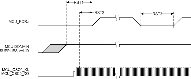
Table 7-6 MCU_PORz Timing Requirements see Figure 7-10
| NO. | MIN | TYP | MAX | UNIT | ||
|---|---|---|---|---|---|---|
| RST1 | th(MCUD_SUPPLIES_VALID - MCU_PORz) | Hold time, MCU_PORz active (low) at Power-up after all MCU DOMAIN supplies valid (using external crystal) | N + 1200(2) | 9500000 | ns | |
| RST2 | Hold time, MCU_PORz active (low) at Power-up after all MCU DOMAIN supplies(1) valid and external clock stable (using external LVCMOS oscillator) | 1200 | ns | |||
| RST3 | tw(MCU_PORzL) | Pulse Width minimum, MCU_PORz low after Power-up (without removal of Power or system reference clock MCU_OSC0_XI/XO) | 1200 | ns | ||
(1) For definition of the MCU DOMAIN
supplies, see the Combined MCU and Main Domains Power-Up sequence TBD.
(2) N = oscillator start-up time
 Figure 7-10 MCU_PORz Timing Requirements
 Table 7-7 PORz Timing Requirements see Figure 7-11
| NO. | MIN | MAX | UNIT | ||
|---|---|---|---|---|---|
| RST4 | th(MAIND_SUPPLIES_VALID - PORz) | Hold time, PORz active (low) at Power-up after all MAIN DOMAIN supplies1 valid | 1200 | ns | |
| RST5 | tw(PORzL) | Pulse Width minimum, PORz low after Power-up | 1200 | ns | |
- For definition of the MAIN DOMAIN supplies, see the Combined MCU and Main Domains Power-Up sequence TBD.
 Figure 7-11 PORz Timing Requirements
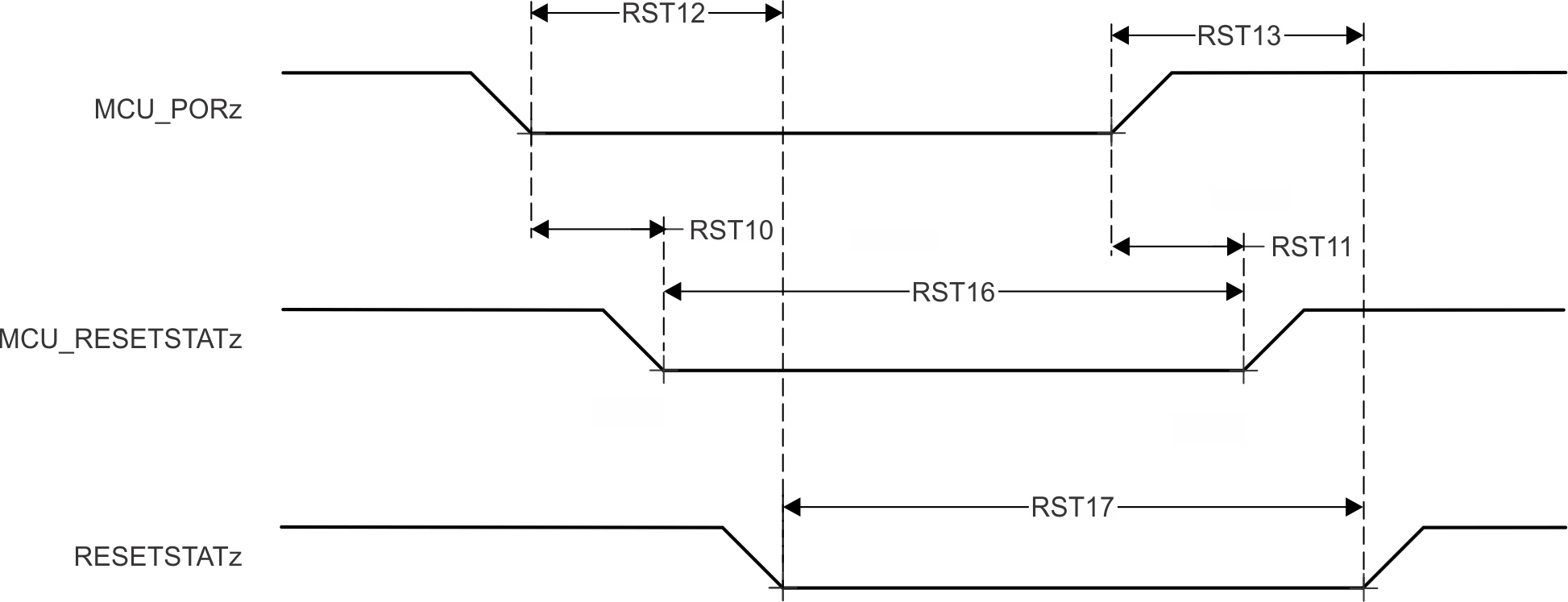
Table 7-8 MCU_PORz initiates; MCU_RESETSTATz, and RESETSTATz
Switching Characteristics see Figure 7-12
| NO. | PARAMETER | MODE | MIN | MAX | UNIT | |
|---|---|---|---|---|---|---|
| RST10 | td(MCU_PORzL-MCU_RESETSTATzL) | Delay time, MCU_PORz active (low) to MCU_RESETSTATz active (low) | 0 | ns | ||
| RST11 | td(MCU_PORzH-MCU_RESETSTATzH) | Delay time, MCU_PORz inactive (high) to MCU_RESETSTATz inactive (high) | POST bypass |
12000*S(1) | ns | |
| RST12 | td(MCU_PORzL-RESETSTATzL) | Delay time, MCU_PORz active (low) to RESETSTATz active (low) | 0 | ns | ||
| RST13 | td(MCU_PORzH-RESETSTATzH) | Delay time, MCU_PORz inactive (high) to RESETSTATz inactive (high) | 14500*S(1) | ns | ||
| RST16 | tw(MCU_RESETSTATzL) | Pulse Width Minimum MCU_RESETSTATz low | 3900*S(1) | ns | ||
| RST17 | tw(RESETSTATzL) | Pulse Width Minimum RESETSTATz low | 2650*S(1) | ns | ||
(1) S = MCU_OSC0_XI/XO clock period.
 Figure 7-12 MCU_PORz initiates; MCU_RESETSTATz,
and RESETSTATz Switching Characteristics
Figure 7-12 MCU_PORz initiates; MCU_RESETSTATz,
and RESETSTATz Switching CharacteristicsTable 7-9 PORz Initiates; PORz_OUT and
RESETSTATz Switching Characteristics see Figure 7-13
| NO. | PARAMETER | MODE | MIN | MAX | UNIT | |
|---|---|---|---|---|---|---|
| RST20 | td(PORzL-RESETSTATzL) | Delay time, PORz active (low) to RESETSTATz active (low) | T(1) | |||
| CTRLMMR_WKUP_POR_RST _CTRL[0].POR_RST_ISO_ DONE_Z = 0 |
0 | ns | ||||
| RST21 | td(PORzH-RESETSTATzH) | Delay time, PORz active (high) to RESETSTATz active (high) | 14500*S(2) | ns | ||
(1) T = Reset Isolation Time (Software
Dependent).
(2) S = MCU_OSC0_XI/XO clock period.
 Figure 7-13 PORz initiates; RESETSTATz Switching
Characteristics
Figure 7-13 PORz initiates; RESETSTATz Switching
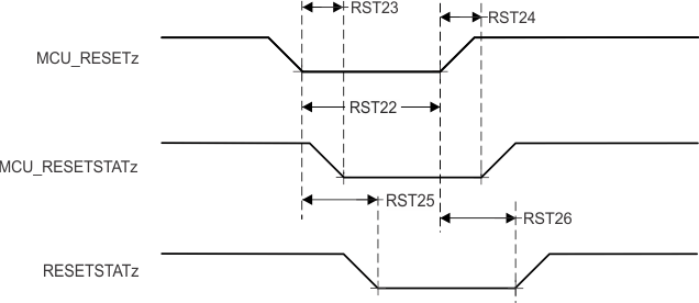
CharacteristicsTable 7-10 MCU_RESETz Timing Requirements see Figure 7-14
| NO. | MIN | MAX | UNIT | ||
|---|---|---|---|---|---|
| RST22 | tw(MCU_RESETzL)(1) | Pulse Width minimum, MCU_RESETz active (low) | 1200 | ns | |
(1) Timing for MCU_RESETz is valid only after
all supplies are valid and MCU_PORz has been asserted for the specified time.
Table 7-11 MCU_RESETz initiates; MCU_RESETSTATz,
and RESETSTATz Switching Characteristics see Figure 7-14
| NO. | PARAMETER | MIN | MAX | UNIT | |
|---|---|---|---|---|---|
| RST23 | td(MCU_RESETzL-MCU_RESETSTATzL) | Delay time, MCU_RESETz active (low) to MCU_RESETSTATz active (low) | 800 | ns | |
| RST24 | td(MCU_RESETzH-MCU_RESETSTATzH) | Delay time, MCU_RESETz inactive (high) to MCU_RESETSTATz inactive (high) | 3900*S(1) | ns | |
| RST25 | td(MCU_RESETzL-RESETSTATzL) | Delay time, MCU_RESETz active (low) to RESETSTATz active (low) | 800 | ns | |
| RST26 | td(MCU_RESETzH-RESETSTATzH) | Delay time, MCU_RESETz inactive (high) to RESETSTATz inactive (high) | 3900*S(1) | ns | |
(1) S = MCU_OSC0_XI/XO clock period.
 Figure 7-14 MCU_RESETz initiates; MCU_RESETSTATz,
and RESETSTATz Timing Requirements and Switching Characteristics
Figure 7-14 MCU_RESETz initiates; MCU_RESETSTATz,
and RESETSTATz Timing Requirements and Switching CharacteristicsTable 7-12 RESET_REQz Timing Requirements see Figure 7-15
| NO. | MIN | MAX | UNIT | ||
|---|---|---|---|---|---|
| RST27 | tw(RESET_REQzL)(1) | Pulse Width minimum, RESET_REQz active (low) | 1200 | ns | |
(1) Timing for RESET_REQz is valid only after
all supplies are valid and MCU_PORz has been asserted for the specified time.
Table 7-13 RESET_REQz initiates; RESETSTATz
Switching Characteristics see Figure 7-15
| NO. | PARAMETER | MODE | MIN | MAX | UNIT | |
|---|---|---|---|---|---|---|
| RST28 | td(RESET_REQzL-RESETSTATzL) | Delay time, RESET_REQz active (low) to RESETSTATz active (low) | software control of SOC_WARMRST_ISO_DONE_Z |
T(1) | ||
| CTRLMMR_WKUP_MAIN_WARM _RST_CTRL[0].SOC_ WARMRST_ISO_DONE_Z = 0 |
740 | ns | ||||
| RST29 | td(RESET_REQzH-RESETSTATzH) | Delay time, RESET_REQz inactive (high) to RESETSTATz inactive (high) | 2650*S(2) | ns | ||
(1) T = Reset Isolation Time (Software
Dependent).
(2) S = MCU_OSC0_XI/XO clock period.
 Figure 7-15 RESET_REQz initiates; RESETSTATz
Timing Requirements and Switching Characteristics
Figure 7-15 RESET_REQz initiates; RESETSTATz
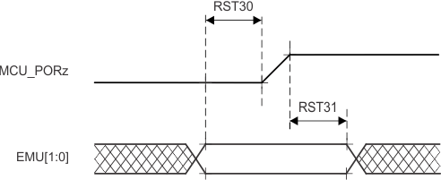
Timing Requirements and Switching CharacteristicsTable 7-14 EMUx Timing Requirements see Figure 7-16
| NO. | MIN | MAX | UNIT | ||
|---|---|---|---|---|---|
| RST30 | tsu(EMUx-MCU_PORz) | Setup time, EMU[1:0] before MCU_PORz inactive (high) | 3*S(1) | ns | |
| RST31 | th(MCU_PORz - EMUx) | Hold time, EMU[1:0] after MCU_PORz inactive (high) | 10 | ns | |
(1) S = MCU_OSC0_XI/XO clock period.
 Figure 7-16 EMUx Timing Requirements
Table 7-15 MCU_BOOTMODE Timing
Requirements see Figure 7-17
| NO. | MIN | MAX | UNIT | ||
|---|---|---|---|---|---|
| RST32 | tsu(MCU_BOOTMODE-MCU_PORz) | Setup time, MCU_BOOTMODE[09:00] before MCU_PORz high | 3*S(1) | ns | |
| RST33 | th(MCU_PORz - MCU_BOOTMODE) | Hold time, MCU_BOOTMODE[09:00] after MCU_ PORz high | 0 | ns | |
(1) S = MCU_OSC0_XI/XO clock period.
 Figure 7-17 MCU_BOOTMODE
Timing Requirements
Figure 7-17 MCU_BOOTMODE
Timing RequirementsTable 7-16 BOOTMODE Timing Requirements see Figure 7-18
| NO. | MIN | MAX | UNIT | ||
|---|---|---|---|---|---|
| RST34 | tsu(BOOTMODE-PORz) | Setup time, BOOTMODE[7:0] before PORz high | 3*S(1) | ns | |
| RST35 | th(PORz - BOOTMODE) | Hold time, BOOTMODE[7:0] after PORz high | 0 | ns | |
(1) S = MCU_OSC0_XI/XO clock period.
 Figure 7-18 BOOTMODE Timing
Requirements