ZHCSES6A February 2016 – March 2016 DRV10970
PRODUCTION DATA.
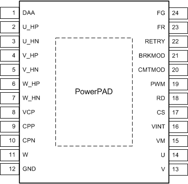
6 Pin Configuration and Functions
PWP Package
24-Pin TSSOP with PowerPAD™
Top View

Pin Functions
| PIN | TYPE | DESCRIPTION | ||
|---|---|---|---|---|
| NAME | NO. | |||
| POWER AND GROUND | ||||
| CPN | 10 | — | Charge pump switching node | Connect a 0.1-µF X7R capacitor rated for VM between CPN and CPP |
| CPP | 9 | — | ||
| GND | 12 | PWR | Device ground | Must be connected to board ground |
| VCP | 8 | — | Charge pump output | Connect a 16-V, 1-µF ceramic capacitor to VM |
| VINT | 16 | PWR | Integrated regulator output | Integrated regulator (typical voltage 5 V) mainly for internal circuits; Provide external power for less than 20 mA. Bypass to GND with a 10-V, 2.2-µF ceramic capacitor |
| VM | 15 | PWR | Power supply | Connect to motor supply voltage; bypass to GND with a 10-µF ceramic capacitor rated for VM |
| CONTROL | ||||
| CS | 17 | — | Current limit setting pin | Connect a resistor to adjust the current limit. |
| DAA | 1 | I | Drive angle adjustment configuration pin | Low: 10° drive angle adjustment High: 5° drive angle adjustment Floating: adaptive drive angle adjustment |
| FG | 24 | O | Frequency indication pin | Open drain Electrical Frequency Output pin. One toggle per electrical cycle. Requires an external pull-up of 3.3-kΩ. |
| FR | 23 | I | Motor direction control | Direction Control Input. When low, phase driving sequence is U → V → W ( U phase is leading V phase by 120°). When high, the phase driving sequence is U → W → V. |
| BRKMOD | 21 | I | Brake mode setting | Low: Coasting mode (phases are tri-stated) High: Brake mode (phases are driven low) |
| PWM | 19 | I | Variable duty cycle PWM input for speed control | Connect to PWM signal. |
| RD | 18 | O | Lock indication pin | Pulled logic low with lock condition; open-drain output requires an external pull-up of 3.3-kΩ |
| RETRY | 22 | I | Auto retry timing configure | Timing adjustable by capacitor |
| CMTMOD | 20 | I | Commutation mode setting | Low: Sinusoidal operation mode with 0° Hall placement High: Sinusoidal operation mode with 30° Hall placement Floating: Trapezoidal operation mode with 30° Hall placement |
| U_HN | 3 | I | U-phase negative Hall input | Differential Hall Sensor negative input for U-phase. Connect to hall sensor negative output. When logic level hall IC is used, tie this pin to VINT/2 level. In single Hall mode, the device uses U-phase hall inputs to drive the motor. |
| U_HP | 2 | I | U-phase positive Hall input | Differential Hall Sensor positive input for U-phase. Connect to hall sensor positive output. When logic level hall IC is used, connect this to hall IC output. In single Hall mode, the device uses U-phase hall inputs to drive the motor. |
| V_HN | 5 | I | V-phase negative Hall input | Differential Hall Sensor negative input for V-phase. Connect to hall sensor negative output. When logic level hall sensor is used, tie this pin to VINT/2 level. In single hall mode, ground this pin. |
| V_HP | 4 | I | V-phase positive Hall input | Differential Hall Sensor positive input for V-phase. Connect to hall sensor positive output. When logic level hall IC is used, connect this to hall IC output. Leave this pin floating to enable single Hall operation. |
| W_HN | 7 | I | W-phase negative Hall input | Differential Hall Sensor negative input for W-phase. Connect to hall sensor negative output. When logic level hall sensor is used, tie this pin to VINT/2 level. In single hall mode, ground this pin. |
| W_HP | 6 | I | W-phase positive Hall input | Differential Hall Sensor positive input for W-phase. Connect to hall sensor positive output. When logic level hall IC is used, connect this to hall IC output. In single hall mode, ground this pin. |
| OUTPUT STAGE | ||||
| U | 14 | O | U phase output | Connect to motor terminal U |
| V | 13 | O | V phase output | Connect to motor terminal V |
| W | 11 | O | W phase output | Connect to motor terminal W |
External Components
| COMPONENT | PIN 1 | PIN 2 | RECOMMENDED |
|---|---|---|---|
| CVM | VM | GND | 10-µF ceramic capacitor rated for VM (if VM = 12 V, 25-V capacitor is suggested, if VM = 18 V, 35-V capacitor is suggested) |
| CVCP | VCP | VM | 16-V, 1-µF ceramic capacitor |
| CSW | CPP | CPN | 0.1-µF X7R capacitor rated for VM |
| CVINT | VINT | GND | 10-V, 2.2-µF ceramic capacitorRotor Lock Detection and Retry |
| CRETRY | RETRY | GND | See Equation 2 for capacitor value |
| RCS | CS | GND | See Current Limit and OCP for resistor value |
| RRD | VCC(1) | RD | >1 kΩ, RD is open-drain output. This component must be pulled up externally. |
| RFG | VCC(1) | FG | >1 kΩ, FG is open-drain output. This component must be pulled up externally. |
(1) VCC is not a pin on the DRV10970. It can be VINT or any other system voltage (for example the 3.3-V or 5-V supply voltage powering the microcontroller). A VCC supply voltage pull-up is required for open-drain outputs RD and FG