| POWER SUPPLIES (VM, VINT) |
| VM |
VM operating voltage |
|
5 |
|
18 |
V |
| IVM |
VM operating supply current |
VM = 12 V, no external load on VINT |
|
3 |
5 |
mA |
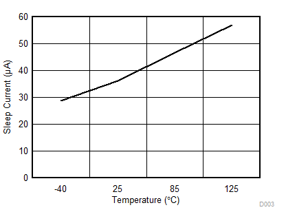
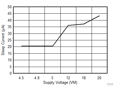
| IVM_SLEEP |
VM supply current during sleep mode |
VM = 5 and 12 V |
|
35 |
50 |
µA |
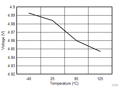
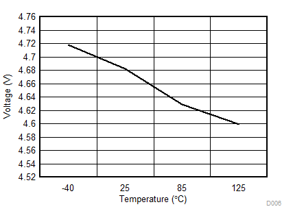
| VINT |
Integrated regulator voltage |
VM = 12 V, 0-mA external load |
4.5 |
5 |
5.5 |
V |
| VM = 12 V, 20-mA external load |
4.5 |
5 |
5.5 |
V |
| VM = 5 V, 0-mA external load |
4.5 |
4.8 |
5 |
V |
| VM = 5 V, 20-mA external load |
4.5 |
4.8 |
5 |
V |
| VGND-BGND |
Ground potential difference between GND pin to PCB ground |
|
|
|
300 |
mV |
| CHARGE PUMP (VCP, CPP, CPN) |
| VCP |
VCP operating voltage |
VM = 5 V, less than 1-mA load |
9 |
10 |
11 |
V |
| VM = 12 V, less than 1-mA load |
16 |
18 |
19.5 |
V |
| VM = 18 V, less than 1-mA load |
22 |
24 |
25.5 |
V |
| CONTROL INPUTS (PWM) |
| VIL-PWM |
PWM Input logic low voltage |
VM = 5 V and VM = 12 V |
0 |
|
0.8 |
V |
| VIH-PWM |
PWM Input logic high voltage |
VM = 5 V and VM = 12 V |
2.4 |
|
5.3 |
V |
| VHYS-PWM |
PWM Input logic hysteresis |
VM = 5 V and VM = 12 V |
400 |
|
|
mV |
| RPU-PWM |
Internal pullup resistance |
VM = 5 V and VM = 12 V |
70 |
100 |
120 |
kΩ |
| RPU-PWM-SL |
Internal pullup resistance in sleep mode |
VM = 5 V and VM = 12 V, sleep mode |
1 |
2 |
2.5 |
MΩ |
| CONTROL INPUTS (RETRY) |
| IRETRY-SINK |
Retry timing set sinking current |
VM = 5 V and 12 V |
9 |
10 |
11 |
µA |
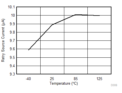
| IRETRY-SOURCE |
Retry timing set sourcing current |
VM = 5 V and 12 V |
9 |
10 |
11 |
µA |
| VRETRY_H |
Retry comparator high threshold |
VM = 5 V and 12 V |
1.1 |
1.2 |
1.3 |
V |
| VRETRY_L |
Retry comparator low threshold |
VM = 5 V and 12 V |
0.55 |
0.6 |
0.65 |
V |
| CONTROL INPUTS (FR, DAA, CMTMOD, BRKMOD) |
| VIL |
Digital input logic low voltage |
VM = 5 V and 12 V |
0 |
|
0.8 |
V |
| VIH |
Digital input logic high voltage |
VM = 5 V and 12 V |
2.2 |
|
5.3 |
V |
| VIFLOATING |
Digital input floating voltage |
VM = 5 V and 12 V |
24% × VINT |
|
36% × VINT |
V |
| RPD-FR |
FR pin Internal pulldown resistance |
VM = 5 V and 12 V |
160 |
200 |
240 |
kΩ |
| RPD-BRKMOD |
BRKMOD pin Internal pulldown resistance |
VM = 5 V and 12 V |
160 |
200 |
240 |
kΩ |
| CONTROL OUTPUTS (RD, FG) |
| IOSINK |
OD output pin sink current |
VO = 0.3 V |
3.5 |
|
|
mA |
| IOSHORT |
OD output pin short current limit |
VO = 12 V |
|
10 |
25 |
mA |
| HALL INPUT COMPARATOR |
| VHR |
Hall input rising |
Zero to positive peak including offset. TA = –40°C, 25°C, 125°C |
0 |
5 |
10 |
mV |
| VHF |
Hall input falling |
Zero to negative peak including offset TA = –40°C, 25°C, 125°C |
–10 |
–5 |
0 |
mV |
| VHALL_HYS |
Hall input hysteresis |
VHP-VHN TA = –40°C, 25°C, 125°C |
5 |
|
12 |
mV |
| Vcom |
Common mode voltage |
VM = 5.5 V – 18 V |
0.3 |
|
4.3 |
V |
| VM = 5 V – 5.5 V |
0.3 |
|
3.8 |
V |
| Finput |
Input frequency range |
|
0 |
|
1000 |
Hz |
| UVLO |
| VUVLO-VM-THR |
UVLO threshold voltage on VM, rising |
|
3.8 |
4 |
4.5 |
V |
| VUVLO-VM-THF |
UVLO threshold voltage on VM, falling |
|
3.6 |
3.8 |
4.25 |
V |
| VUVLO-VM-HYS |
VM UVLO comparator hysteresis |
|
40 |
|
200 |
mV |
| VUVLO-VINT-THR |
VINT UVLO rise threshold |
|
4.1 |
4.2 |
4.5 |
V |
| VUVLO-VINT-THF |
VINT UVLO fall threshold |
|
3.8 |
4 |
4.2 |
V |
| VUVLO-VINT-HYS |
VINT UVLO comparator hysteresis |
|
100 |
|
300 |
mV |
| INTEGRATED MOSFET |
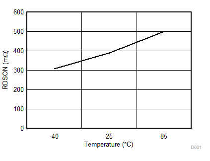
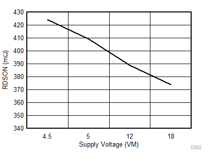
| RDSON |
Series resistance (H + L) |
VM = 12 V, VCP = 19 V, IOUT = 1.5 A |
|
0.4 |
0.6 |
Ω |
| CURRENT LIMIT AND OVER CURRENT PROTECTION (OCP) |
| ILIM |
Current limit threshold |
VM = 12 V, Rcs = 20 kΩ |
1.3 |
1.5 |
1.7 |
A |
| VILIM_THR |
Current limit circuit comparator threshold |
VM = 12 V |
1.15 |
1.2 |
1.25 |
V |
| ACL |
Current limit attenuation factor |
VM = 12 V |
22000 |
25000 |
28000 |
A/A |
| IOCP |
Over current protection threshold. Magnitude of phase current at which driver stage is disabled to protect the device. |
VM = 5 V and 12 V |
3 |
|
5 |
A |
| SLEEP MODE TIMING |
| TSLEEP_EN |
Minimum PWM low time to recognize a sleep command. |
VM = 12 V |
1.2 |
|
|
ms |
| TSLEEP_EX |
Minimum PWM high to exit from sleep mode. |
VM = 12 V |
2 |
|
|
µs |
| THERMAL SHUTDOWN |
| TSDN_TR |
Shut down temperature threshold |
Shut down triggering temperature |
150 |
160 |
170 |
°C |
| TSDN_RS |
Shut down resume temperature |
Shut down resume temperature |
140 |
150 |
160 |
°C |
| TSDN_HYS |
Shut down temperature hysteresis |
Shut down temperature hysteresis |
5 |
10 |
15 |
°C |
| LOCK DETECT |
| tLOCK_EN |
Lock detect time |
|
0.6 |
0.7 |
0.8 |
s |
| tLOCK_EX |
Lock release time |
Retry capacitor = 0.33 uF |
4 |
5 |
6 |
s |
