ZHCSDA7G July 2014 – February 2018 DRV10983
PRODUCTION DATA.
- 1 特性
- 2 应用
- 3 说明
- 4 修订历史记录
- 5 说明 (续)
- 6 Pin Configuration and Functions
- 7 Specifications
-
8 Detailed Description
- 8.1 Overview
- 8.2 Functional Block Diagram
- 8.3 Feature Description
- 8.4
Device Functional Modes
- 8.4.1 Motor Parameters
- 8.4.2 Starting the Motor Under Different Initial Conditions
- 8.4.3 Motor Start Sequence
- 8.4.4 Start-Up Current Setting
- 8.4.5 Closed Loop
- 8.4.6 Current Limit
- 8.4.7 Lock Detect and Fault Handling
- 8.4.8 AVS Function
- 8.4.9 PWM Output
- 8.4.10 FG Customized Configuration
- 8.4.11
Diagnostics and Visibility
- 8.4.11.1 Motor Status Readback
- 8.4.11.2 Motor Speed Readback
- 8.4.11.3 Motor Electrical Period Readback
- 8.4.11.4 BEMF Constant Readback
- 8.4.11.5 Motor Estimated Position by IPD
- 8.4.11.6 Supply Voltage Readback
- 8.4.11.7 Speed Command Readback
- 8.4.11.8 Speed Command Buffer Readback
- 8.4.11.9 Fault Diagnostics
- 8.5 Register Maps
- 9 Application and Implementation
- 10Power Supply Recommendations
- 11Layout
- 12器件和文档支持
- 13机械、封装和可订购信息
8.3.3 Motor Speed Control
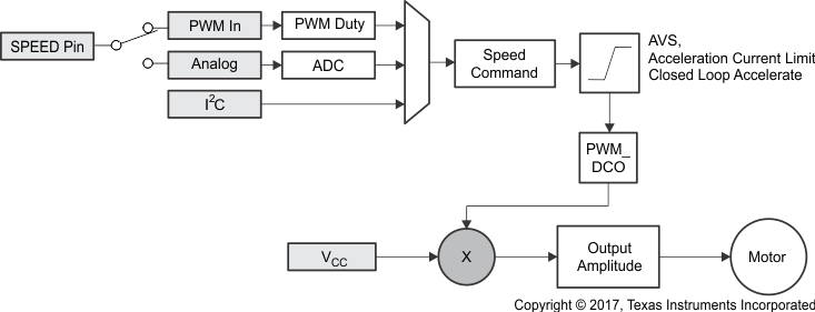
The DRV10983 offers four methods for indirectly controlling the speed of the motor by adjusting the output voltage amplitude. This can be accomplished by varying the supply voltage (VCC) or by controlling the Speed Command. The Speed Command can be controlled in one of three ways. The user can set the Speed Command on the SPEED pin by adjusting either the PWM input (SPEED pin configured for PWM mode) or the analog input (SPEED pin configured for analog mode), or by writing the Speed Command directly through the I2C serial port to SpdCtrl[8:0]. The Speed Command is used to determine the PWM duty cycle output (PWM_DCO) (see Figure 5).
The Speed Command may not always be equal to the PWM_DCO because DRV10983 has implemented the AVS function (see AVS Function), the acceleration current limit function (see Acceleration Current Limit), and the closed loop accelerate function (see Closed Loop Accelerate) to optimize the control performance. These functions can limit the PWM_DCO, which affects the output amplitude.
 Figure 5. Multiplexing the Speed Command to the Output Amplitude Applied to the Motor
The output voltage amplitude applied to the motor is accomplished through sine wave modulation so that the phase-to-phase voltage is sinusoidal.
When any phase is measured with respect to ground, the waveform is sinusoidally coupled with third-order harmonics. This encoding technique permits one phase to be held at ground while the other two phases are pulse-width modulated. Figure 6 and Figure 7 show the sinusoidal encoding technique used in the DRV10983.
 Figure 6. PWM Output and the Average Value

| Sinusoidal voltage from phase to phase | Sinusoidal voltage with third order harmonics from phase to GND |
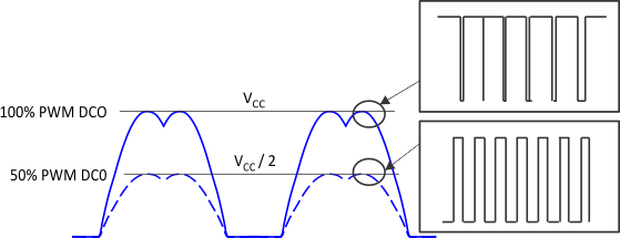
The output amplitude is determined by the magnitude of VCC and the PWM duty cycle output (PWM_DCO). The PWM_DCO represents the peak duty cycle that is applied in one electrical cycle. The maximum amplitude is reached when PWM_DCO is at 100%. The peak output amplitude is VCC. When the PWM_DCO is at 50%, the peak amplitude is VCC / 2 (see Figure 8).
 Figure 8. Output Voltage Amplitude Adjustment