ZHCSDA7G July 2014 – February 2018 DRV10983
PRODUCTION DATA.
- 1 特性
- 2 应用
- 3 说明
- 4 修订历史记录
- 5 说明 (续)
- 6 Pin Configuration and Functions
- 7 Specifications
-
8 Detailed Description
- 8.1 Overview
- 8.2 Functional Block Diagram
- 8.3 Feature Description
- 8.4
Device Functional Modes
- 8.4.1 Motor Parameters
- 8.4.2 Starting the Motor Under Different Initial Conditions
- 8.4.3 Motor Start Sequence
- 8.4.4 Start-Up Current Setting
- 8.4.5 Closed Loop
- 8.4.6 Current Limit
- 8.4.7 Lock Detect and Fault Handling
- 8.4.8 AVS Function
- 8.4.9 PWM Output
- 8.4.10 FG Customized Configuration
- 8.4.11
Diagnostics and Visibility
- 8.4.11.1 Motor Status Readback
- 8.4.11.2 Motor Speed Readback
- 8.4.11.3 Motor Electrical Period Readback
- 8.4.11.4 BEMF Constant Readback
- 8.4.11.5 Motor Estimated Position by IPD
- 8.4.11.6 Supply Voltage Readback
- 8.4.11.7 Speed Command Readback
- 8.4.11.8 Speed Command Buffer Readback
- 8.4.11.9 Fault Diagnostics
- 8.5 Register Maps
- 9 Application and Implementation
- 10Power Supply Recommendations
- 11Layout
- 12器件和文档支持
- 13机械、封装和可订购信息
8.4.1.1 Motor Phase Resistance
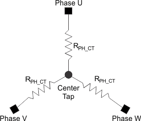
For a wye-connected motor, the motor phase resistance refers to the resistance from the phase output to the center tap, RPH_CT (see Figure 9).
 Figure 9. Wye-Connected Motor Phase Resistance
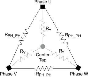
For a delta-connected motor, the motor phase resistance refers to the equivalent phase to center tap in the wye configuration, which is represented as RY. RPH_CT = RY (see Figure 10).
For both the delta-connected motor and the wye-connected motor, calculating the equivalent RPH_CT is easy by measuring the resistance between two phase terminals (RPH_PH), and then dividing this value by two as shown in Equation 1.
 Figure 10. Delta-Connected Motor and the Equivalent Wye Connections
The motor phase resistance (RPH_CT) must be converted to a 7-bit digital register value Rm[6:0] to program the motor phase resistance value. The digital register value can be determined as follows:
- Convert the motor phase resistance (RPH_CT) to a digital value where the LSB is weighted to represent 9.67 mΩ: Rmdig = RPH_CT / 0.00967.
- Encode the digital value such that Rmdig = Rm[3:0] << Rm[6:4].
The maximum resistor value, RPH_CT, that can be programmed for the DRV10983 is 18.5 Ω, which represents Rmdig = 1920 and an encoded Rm[6:0] value of 0x7Fh. The minimum resistor the DRV10983 supports is 0.029 Ω, RPH_CT, which represents Rmdig = 3.
For convenience, the encoded value for Rm[6:0] can also be obtained from Table 2.
Table 2. Motor Phase Resistance Look-Up Table
| RPH_CT (Ω) | RM[6:0] | HEX | RPH_CT (Ω) | RM[6:0] | HEX | RPH_CT (Ω) | RM[6:0] | HEX | ||
|---|---|---|---|---|---|---|---|---|---|---|
| 0.0000 | 000 0000 | 00 | 0.309 | 010 1000 | 28 | 2.47 | 101 1000 | 58 | ||
| 0.0097 | 000 0001 | 01 | 0.348 | 010 1001 | 29 | 2.78 | 101 1001 | 59 | ||
| 0.0193 | 000 0010 | 02 | 0.387 | 010 1010 | 2A | 3.09 | 101 1010 | 5A | ||
| 0.029 | 000 0011 | 03 | 0.426 | 010 1011 | 2B | 3.4 | 101 1011 | 5B | ||
| 0.0387 | 000 0100 | 04 | 0.464 | 010 1100 | 2C | 3.71 | 101 1100 | 5C | ||
| 0.0484 | 000 0101 | 05 | 0.503 | 010 1101 | 2D | 4.02 | 101 1101 | 5D | ||
| 0.058 | 000 0110 | 06 | 0.542 | 010 1110 | 2E | 4.33 | 101 1110 | 5E | ||
| 0.0677 | 000 0111 | 07 | 0.58 | 010 1111 | 2F | 4.64 | 101 1111 | 5F | ||
| 0.0774 | 000 1000 | 08 | 0.619 | 011 1000 | 38 | 4.95 | 110 1000 | 68 | ||
| 0.087 | 000 1001 | 09 | 0.696 | 011 1001 | 39 | 5.57 | 110 1001 | 69 | ||
| 0.0967 | 000 1010 | 0A | 0.773 | 011 1010 | 3A | 6.18 | 110 1010 | 6A | ||
| 0.106 | 000 1011 | 0B | 0.851 | 011 1011 | 3B | 6.8 | 110 1011 | 6B | ||
| 0.116 | 000 1100 | 0C | 0.928 | 011 1100 | 3C | 7.42 | 110 1100 | 6C | ||
| 0.126 | 000 1101 | 0D | 1 | 011 1101 | 3D | 8.04 | 110 1101 | 6D | ||
| 0.135 | 000 1110 | 0E | 1.08 | 011 1110 | 3E | 8.66 | 110 1110 | 6E | ||
| 0.145 | 000 1111 | 0F | 1.16 | 011 1111 | 3F | 9.28 | 110 1111 | 6F | ||
| 0.155 | 001 1000 | 18 | 1.23 | 100 1000 | 48 | 9.9 | 111 1000 | 78 | ||
| 0.174 | 001 1001 | 19 | 1.39 | 100 1001 | 49 | 11.1 | 111 1001 | 79 | ||
| 0.193 | 001 1010 | 1A | 1.54 | 100 1010 | 4A | 12.3 | 111 1010 | 7A | ||
| 0.213 | 001 1011 | 1B | 1.7 | 100 1011 | 4B | 13.6 | 111 1011 | 7B | ||
| 0.232 | 001 1100 | 1C | 1.85 | 100 1100 | 4C | 14.8 | 111 1100 | 7C | ||
| 0.251 | 001 1101 | 1D | 2.01 | 100 1101 | 4D | 16 | 111 1101 | 7D | ||
| 0.271 | 001 1110 | 1E | 2.16 | 100 1110 | 4E | 17.3 | 111 1110 | 7E | ||
| 0.29 | 001 1111 | 1F | 2.32 | 100 1111 | 4F | 18.5 | 111 1111 | 7F |