ZHCSAH5A November   2012  – November 2014 DRV11873

PRODUCTION DATA.  

  1. 特性
  2. 应用范围
  3. 说明
  4. 简化电路原理图
  5. 修订历史记录
  6. Pin Configuration and Functions
  7. Specifications
    1. 7.1 Absolute Maximum Ratings
    2. 7.2 Handling Ratings
    3. 7.3 Recommended Operating Conditions
    4. 7.4 Thermal Information
    5. 7.5 Electrical Characteristics
    6. 7.6 Typical Characteristics
  8. Detailed Description
    1. 8.1 Overview
    2. 8.2 Functional Block Diagram
    3. 8.3 Feature Description
      1. 8.3.1  Speed Control
      2. 8.3.2  Frequency Generator
      3. 8.3.3  FS Setting
      4. 8.3.4  Lock Protection and RD Output
      5. 8.3.5  Reverse Spin Control FR
      6. 8.3.6  5-V LDO
      7. 8.3.7  Overcurrent Protection
      8. 8.3.8  UVLO
      9. 8.3.9  Thermal Shutdown
      10. 8.3.10 Anti-Voltage Surge (AVS)
    4. 8.4 Device Functional Modes
      1. 8.4.1 Startup
      2. 8.4.2 Closed Loop Control
      3. 8.4.3 AVS Protection
  9. Application and Implementation
    1. 9.1 Application Information
    2. 9.2 Typical Application
      1. 9.2.1 Design Requirements
      2. 9.2.2 Detailed Design Procedure
      3. 9.2.3 Application Curves
  10. 10Power Supply Recommendations
  11. 11Layout
    1. 11.1 Layout Guidelines
    2. 11.2 Layout Example
  12. 12器件和文档支持
    1. 12.1 商标
    2. 12.2 静电放电警告
    3. 12.3 术语表
  13. 13机械、封装和可订购信息

封装选项

机械数据 (封装 | 引脚)
散热焊盘机械数据 (封装 | 引脚)
订购信息

Specifications

Absolute Maximum Ratings

over operating free-air temperature (unless otherwise noted)
MIN MAX UNIT
Input voltage(1) VCC –0.3 20 V
CS –0.3 3.6
PWMIN, FS, FR –0.3 6
GND –0.3 0.3
COM –1 20
Output voltage(1) U, V, W –1 20 V
FG, RD –0.3 20
VCP –0.3 25
CPN –0.3 20
CPP –0.3 25
V5 –0.3 6
TJ Operating junction temperature –40 125 °C
Voltage values are with respect to the network ground terminal unless otherwise noted.

Handling Ratings

MIN MAX UNIT
Tstg Storage temperature range –55 150 °C
V(ESD) Electrostatic discharge Human body model (HBM), per ANSI/ESDA/JEDEC JS-001, all pins(1) –4000 4000 V
Charged device model (CDM), per JEDEC specification JESD22-C101, all pins(2) –1000 1000
Machine model (MM) –200 200
JEDEC document JEP155 states that 500-V HBM allows safe manufacturing with a standard ESD control process.
JEDEC document JEP157 states that 250-V CDM allows safe manufacturing with a standard ESD control process.

Recommended Operating Conditions

over operating free-air temperature range (unless otherwise noted)
MIN MAX UNIT
Supply voltage VCC 5 16 V
Voltage range U, V, W –0.7 17 V
COM –0.1 17
FG, RD –0.1 16
PGND, GND –0.1 0.1
VCP –0.1 22
CPP –0.1 22
CPN –0.1 16
V5 –0.1 5.5
PWMIN, FR, FS –0.1 5.5
TJ Operating junction temperature –40 125 V

Thermal Information

THERMAL METRIC(1) DRV11873 UNIT
PWP
16 PINS
RθJA Junction-to-ambient thermal resistance 39.4 °C/W
RθJC(top) Junction-to-case (top) thermal resistance 30.3
RθJB Junction-to-board thermal resistance 25.6
ψJT Junction-to-top characterization parameter 0.5
ψJB Junction-to-board characterization parameter 10.2
RθJC(bot) Junction-to-case (bottom) thermal resistance 3.6
For more information about traditional and new thermal metrics, see the IC Package Thermal Metrics application report, SPRA953.

Electrical Characteristics

over recommended operating free-air temperature (unless otherwise noted)
PARAMETER TEST CONDITIONS MIN TYP MAX UNIT
SUPPLY CURRENT
IVCC Supply current TA = 25°C; PWM = VCC; VCC = 12 V 2.7 5 mA
UVLO
VVUVLO-th_r UVLO threshold voltage Rise threshold, TA = 25°C 4.3 4.6 V
VUVLO-th_f UVLO threshold voltage Fall threshold, TA = 25°C 3.9 4.1 V
VUVLO-thhys UVLO threshold voltage hysteresis TA = 25°C 100 200 300 mV
INTEGRATED MOSFET
RDSON Series resistance (H + L) TA = 25°C; VCC = 12 V; VCP = 19 V;
IOUT = 1.5 A
0.45 0.6 Ω
PWM
VPWM-IH High-level input voltage VCC ≥ 4.5 V 2.7 V
VPWM-IL Low-level input voltage VCC ≥ 4.5 V 0.8 V
ƒPWM PWM input frequency 7 100 kHz
IPWM-SOURCE PWM source current 35 50 65 µA
FG
IFG-SINK FG pin sink current VFG = 0.3 V 5 mA
IFG-short FG pin short current limit VFG = 12 V 20 25 mA
RD
IRD-SINK RD pin sink current VRD = 0.3 V 5 mA
IRD-short RD pin short current limit VRD = 12 V 20 25 mA
FR and FS
VFR-IH High-level input voltage VCC ≥ 4.5 V 2.3 V
VFR-IL Low-level input voltage VCC ≥ 4.5 V 0.8 V
VFS-th FS set threshold voltage VCC ≥ 4.5 V 2.3 0.8 V
V5
V5 5-V LDO voltage VCC = 12 V 4.75 5 5.25 V
IV5 5-V LDO load current VCC = 12 V 20 mA
LOCK PROTECTION
tLOCK-ON Lock detect time FS = 0 0.875 1.25 1.625 s
FS = 1 0.437 0.625 0.812
tLOCK-OFF Lock release time FS = 0 4.375 6.25 8.125 s
FS = 1 2.187 3.125 4.06
CURRENT LIMIT
Current limit CS pin to GND resistor = 3.3 kΩ 1.7 2 2.3 A
THERMAL SHUTDOWN
TSDN Shutdown temperature threshold Shutdown temperature 160 °C
Hysteresis 10

Typical Characteristics

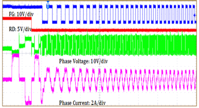
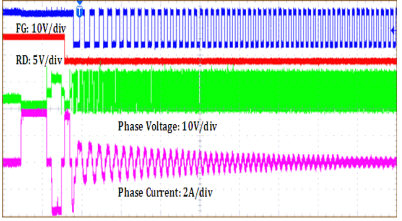
DRV11873 start_up_100_lws237.gif
Input voltage = 12 V PWM duty = 100% FS = 1
t = 20 ms/div
Figure 1. Start Up at 100% Duty
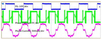
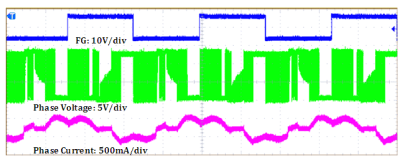
DRV11873 nrml_op_100_lws237.gif
Input voltage = 12 V PWM duty = 100% FS = 1
t = 800 µs/div
Figure 3. Normal Operation at 100% Duty
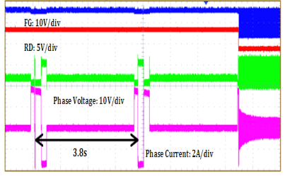
DRV11873 lock_protection_lws237.gif
Input voltage = 12 V PWM duty = 100% FS = 1
t = 1 s/div
Figure 5. Lock Protection
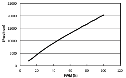
DRV11873 fast_motor_lws237.gif
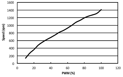
Figure 7. Fast Motor RPM vs Duty, FS = 1
DRV11873 fast_motor_vs_voltage_lws237.gif
Figure 9. Fast Motor RPM vs Voltage, FS = 1
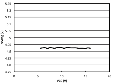
DRV11873 ldo_line_reg_lws237.gif
Figure 11. 5-V LDO Line Regulation
DRV11873 start_up_10_lws237.gif
Input voltage = 12 V PWM duty = 10% FS = 1
t = 40 ms/div
Figure 2. Start Up at 10% Duty
DRV11873 nrml_op_50_lws237.gif
Input voltage = 12 V PWM duty = 50% FS = 1
t = 800 µs/div
Figure 4. Normal Operation at 50% Duty
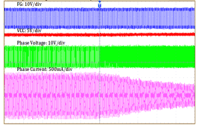
DRV11873 avs_op_lws237.gif
Input voltage = 12 V PWM duty switch from 100% to 20%
t = 20 ms/div FS = 1
Figure 6. AVS Operation
DRV11873 slow_motor_lws237.gif
Figure 8. Slow Motor RPM vs Duty, FS = 0
DRV11873 slow_motor_vs_voltage_lws237.gif
Figure 10. Slow Motor RPM vs Voltage, FS = 0
DRV11873 ldo_load_reg_lws237.gif
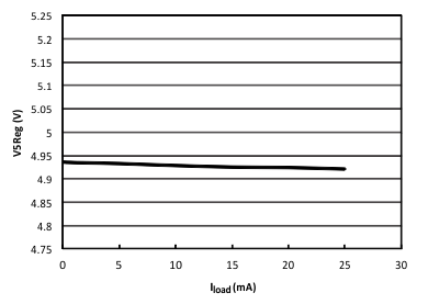
Figure 12. 5-V LDO Load Regulation