ZHCSFA9A June 2016 – July 2016 DRV2511-Q1
PRODUCTION DATA.
- 1 特性
- 2 应用
- 3 说明
- 4 修订历史记录
- 5 Pin Configuration and Functions
- 6 Specifications
- 7 Detailed Description
- 8 Application and Implementation
- 9 Power Supply Recommendations
- 10Layout
- 11器件和文档支持
- 12机械、封装和可订购信息
5 Pin Configuration and Functions
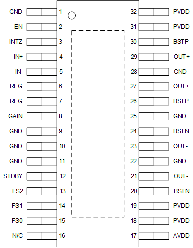
DAP Package
32-Pin HTSSOP
Top View

Pin Functions
| PIN | TYPE | DESCRIPTION | |
|---|---|---|---|
| NAME | NO. | ||
| GND | 1, 9, 10, 11, 22, 25, 28 | P | Ground. |
| EN | 2 | I | Device enable pin. |
| INTZ | 3 | O | General fault reporting. Open drain. INTZ = High, normal operation INTZ = Low, fault condition |
| IN+ | 4 | I | Positive differential input. |
| IN- | 5 | I | Negative differential input. |
| REG | 6, 7 | P | Internally generated gate voltage supply. Not to be used as a supply or connected to any component other than a 1 µF X7R ceramic decoupling capacitor and the MODE resistor divider. |
| GAIN | 8 | I | Selects Gain. |
| STDBY | 12 | I | Standby pin. |
| FS2 | 13 | I | Output switching frequency selection. |
| FS1 | 14 | I | Output switching frequency selection. |
| FS0 | 15 | I | Output switching frequency selection. |
| N/C | 16 | N/C | Pin should be left floating. |
| AVDD | 17 | P | Analog Supply, can be connected to VBAT for single power supply operation. |
| PVDD | 18, 19, 31, 32 | P | Power supply. |
| BSTN | 20, 24 | P | Boot strap for negative output, connect to 220 nF X5R, or better ceramic cap to OUT-. |
| OUT- | 21, 23 | O | Negative output. |
| BSTP | 26, 30 | P | Boot strap for positive output, connect to 220 nF X5R, or better ceramic cap to OUT+. |
| OUT+ | 27, 29 | O | Positive output. |
| Thermal Pad or PowerPAD™ |
G | Connect to GND for best system performance. If not connected to GND, leave floating. | |