ZHCSFA9A June 2016 – July 2016 DRV2511-Q1
PRODUCTION DATA.
- 1 特性
- 2 应用
- 3 说明
- 4 修订历史记录
- 5 Pin Configuration and Functions
- 6 Specifications
- 7 Detailed Description
- 8 Application and Implementation
- 9 Power Supply Recommendations
- 10Layout
- 11器件和文档支持
- 12机械、封装和可订购信息
7 Detailed Description
7.1 Overview
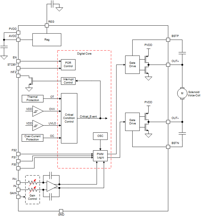
The DRV2511-Q1 device is a high current haptic driver specifically designed for inductive loads, such as solenoids and voice coils.
The output stage consists of a full H-bridge capable of delivering 8 A of peak current.
The design uses an ultra-efficient switching output technology developed by Texas Instruments, but with features added for the automotive industry. The DRV2511-Q1 device provides protection functions such as undervoltage lockout, over-current protection and over-temperature protection. This technology allows for reduced power consumption, reduced heat, and reduced peak currents in the electrical system.
The DRV2511-Q1 device is automotive qualified.
7.2 Functional Block Diagram

7.3 Feature Description
7.3.1 Analog Input and Configurable Pre-amplifier
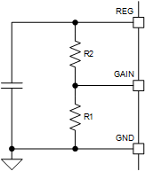
The DRV2511-Q1 device features a differential input stage that cancels common-mode noise that appears on the inputs. The DRV2511-Q1 device also features four gain settings that are configurable via external resistors.
Table 1. Gain Configuration Table
| GAIN | R1 | R2 | INPUT IMPEDANCE |
|---|---|---|---|
| 20 dB | 5.6 kΩ | open | 60 kΩ |
| 26 dB | 20 kΩ | 100 kΩ | 30 kΩ |
| 32 dB | 39 kΩ | 100 kΩ | 15 kΩ |
| 36 dB | 47 kΩ | 75 kΩ | 9 kΩ |
 Figure 3. Gain Configuration
7.3.2 Pulse-Width Modulator (PWM)
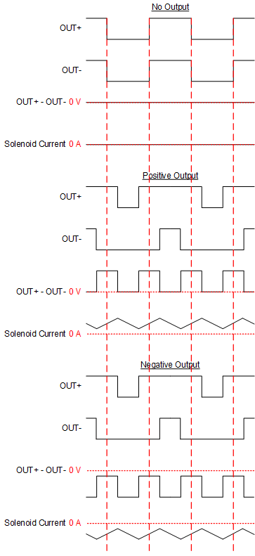
The DRV2511-Q1 device features BD modulation scheme with high bandwidth, low noise, low distortion, and excellent stability.
The BD modulation scheme allows for smaller ripple currents through the load. Each output switches from 0 V to the supply voltage. With no input, the OUT+ and OUT- pins are in phase with each other so that there is little or no current in the load. For positive differential inputs, the duty cycle of OUT+ is greater than 50% and the duty cycle of OUT- is lower than 50% for a positive differential output voltage. The opposite is true for negative differential inputs. The voltage accross the load sits at 0 V throughout most of the switching period, reducing the switching current, which reduces the I2R losses in the load.
 Figure 4. BD Mode Modulation
7.3.3 Designed for low EMI
The DRV2511-Q1 device design has minimal parasitic inductances due to the short leads on the package. This dramatically reduces EMI that results from current passing from the die to the system PCB. The design incorporates circuitry that optimizes output transitions that causes EMI. Follow the recommended design requirements in the Design Requirements section.
7.3.4 Device Protection Systems
The DRV2511-Q1 device features a complete set of protection circuits carefully designed to protect the device against permanent failures due to shorts, over-temperature, over-voltage, and under-voltage scenarios. The INTZ pin signals if an error is detected.
Table 2. Fault Reporting Table
| FAULT | TRIGGERING CONDITION | INTZ | ACTION | LATCH? |
|---|---|---|---|---|
| Over-current | Output short or short to PVDD or GND | pulled low | output in high impedance | Latched |
| Over-temperature | Tj > 150 ºC | pulled low | output in high impedance | Latched |
| Under-voltage | PVDD < 4.5 V | - | output in high impedance | Self-clearing |
| Over-voltage | PVDD > 27 V | - | output in high impedance | Self-clearing |
When the "Latched" conditions happen, the device must be reset with the EN signal in order to clear the fault. If automatic recovery from these conditions is desired, connect the INTZ pin directly to the EN pin. This allows the INTZ pin function to automatically drive the EN pin low which clears the latched condition.
7.4 Device Functional Modes
The DRV2511-Q1 device has multiple power states to optimize power consumption.
7.4.1 Operation in Shutdown Mode
The NRST pin of the DRV2511-Q1 device puts the device in a shutdown mode. When NRST is asserted (logic low), all internal blocks of the device are off to achieve ultra low power.
7.4.2 Operation in Standby Mode
The STDBY pin of the DRV2511-Q1 device puts the device in a standby mode. When STDBY is asserted (logic high), some internal blocks of the device are off to achieve low power while preserving the ability to wake up quickly to achieve low latency waveform playback.
7.4.3 Operation in Active Mode
The DRV2511-Q1 device is in active mode when it has a valid supply, and it is not in either shutdown or standby modes. In this mode the DRV2511-Q1 device is fully on and reproducing at the output the input times the gain.
7.5 Programming
7.5.1 Gain
The DRV2511-Q1 device has a configurable gain that is controlled through external resistors. Please see the Analog Input and Configurable Pre-amplifier section for more details.