ZHCSFA9A June 2016 – July 2016 DRV2511-Q1
PRODUCTION DATA.
- 1 特性
- 2 应用
- 3 说明
- 4 修订历史记录
- 5 Pin Configuration and Functions
- 6 Specifications
- 7 Detailed Description
- 8 Application and Implementation
- 9 Power Supply Recommendations
- 10Layout
- 11器件和文档支持
- 12机械、封装和可订购信息
8 Application and Implementation
NOTE
Information in the following applications sections is not part of the TI component specification, and TI does not warrant its accuracy or completeness. TI’s customers are responsible for determining suitability of components for their purposes. Customers should validate and test their design implementation to confirm system functionality.
8.1 Application Information
The DRV2511-Q1 device is a high-efficiency driver for inductive loads, such as solenoids and voice-coils. The typical use of the device is on haptic applications where short, strong waveforms are desired to create a haptic event that will be coming from the application processor.
8.2 Typical Applications
8.2.1 Single-Ended Source
To use the DRV2511-Q1 with a single-ended source, apply either a voltage divider to bias INB to 3 V, tie to GND or use a 0.1-μF cap from INB to GND to have the device self bias. Apply the single-ended signal to the INA pin.
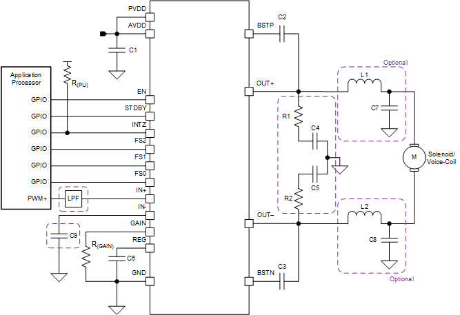 Figure 5. Typical Application Schematic
8.2.1.1 Design Requirements
For most applications the following component values found in Table 3 below can be used.
Table 3. Component Requirements Table
| COMPONENT | DESCRIPTION | SPECIFICATION | TYPICAL VALUE |
|---|---|---|---|
| C1 | Supply capacitor | Capacitance | 22 µF and 0.1 µF for PVDD & AVDD |
| C2/C3 | Boost capacitor | Capacitance | 0.22 µF |
| C4/C5 | Output snubber capacitor | Capacitance | 470 pF |
| C6 | Regulator capacitor | Capacitance | 1 µF |
| C9 | Input decoupling capacitor | Capacitance | 0.1 µF |
| R1/R2 | Output snubber resistor | Resistance | 3.3 Ω |
| R(PU) | Pull-up resistor | Resistance | 100 kΩ |
8.2.1.2 Detailed Design Procedure
8.2.1.2.1 Optional Components
Note that in the diagrams, there are a few optional external components. These optional external components may be needed in the application to meet EMI/EMC standards and specifications by filters necessary frequency spectrums.
8.2.1.2.2 Capacitor Selection
A bulk bypass capacitor should be mounted between VBAT and GND. The capacitance needs to be >22 uF with a X5R or better rating on the power pins to GND. Also include two ceramic capacitors in the ranges of 220 pF to 1 uF and 100 nF to 1 uF. The bootstrap capacitors, BSTA and BSTB, should be 220-nF ceramic capacitors of quality X5R or better rated for at least the maximum rating of the pin.
8.2.1.2.3 Solenoid Selection
The DRV2511-Q1 solenoid driver can accommodate a variety of solenoids. Solenoids should have an equivalent resistance of 1.6 Ω or greater. Solenoids with lower resistances are prone to driving high currents. A maximum peak current of 8-A should not be exceeded. The DRV2511-Q1 will go into a shutdown mode to protect itself from overcurrent.
8.2.1.2.4 Output Filter Considerations
The output filter is optional and is mainly for limiting peak currents. A second-order Butterworth low-pass filter with the cut-off frequency set to a few kilohertz should be sufficient. See Equation 2, Equation 3, and Equation 4 for example filter design.


8.2.1.3 Application Curves
These application curves were taken using an HA200 solenoid with a 100-g mass, and the acceleration was measured using the DRV-AAC16-EVM accelerometer. The following scales apply to the graphs:
- Output Differential Voltage scale is shown on the plots at 5-V/div
- Acceleration scale is 5.85-G/div
- Current scale is 2-A/div
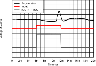 Figure 6. Voltage and Acceleration vs Time (Input Square Wave)
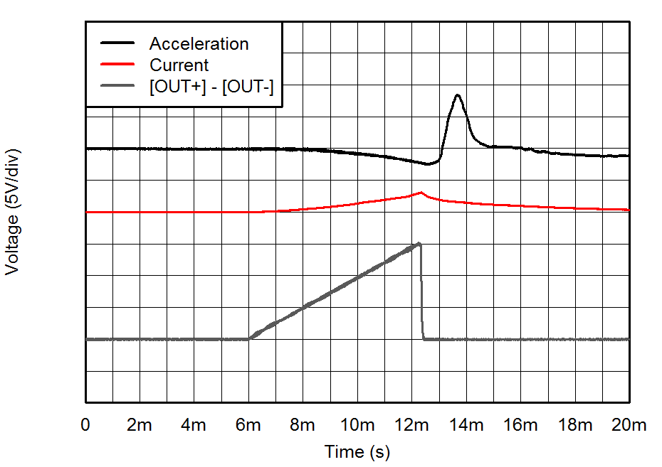 Figure 8. Voltage and Acceleration vs Time (Ramp Wave)
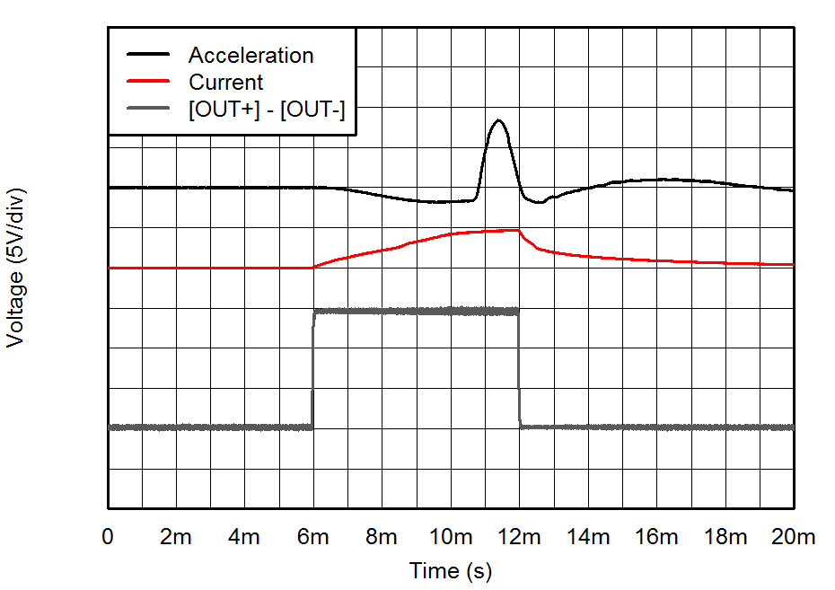 Figure 7. Voltage and Acceleration vs Time (Square Wave)
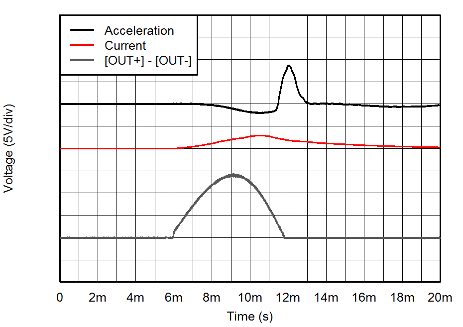 Figure 9. Voltage and Acceleration vs Time (1/2 Sine Wave)
8.2.1.4 Differential Input Diagram
To use the DRV2511-Q1 with a differential input source, apply both inputs differentially from a control source (GPIO, DAC, etc...).
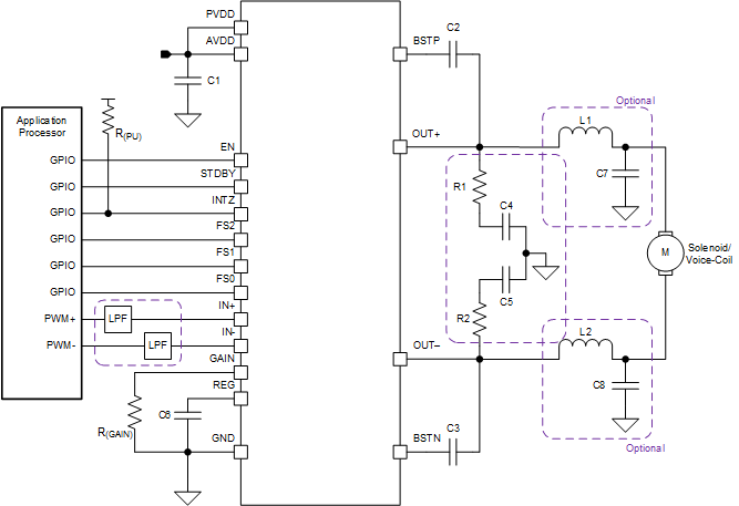 Figure 10. Typical Application Schematic