ZHCS343C May 2012 – January 2023 DRV2665
PRODUCTION DATA
- 1
- 1 特性
- 2 应用
- 3 说明
- 4 Revision History
- 5 Pin Configuration and Functions
- 6 Specifications
-
7 Detailed Description
- 7.1 Overview
- 7.2 Functional Block Diagram
- 7.3
Feature Description
- 7.3.1 Support for Haptic Piezo Actuators
- 7.3.2 Flexible Front End Interface
- 7.3.3 Ramp Down Behavior
- 7.3.4 Low Latency Startup
- 7.3.5 Low Power Standby Mode
- 7.3.6 Device Reset
- 7.3.7 Amplifier Gain
- 7.3.8 Adjustable Boost Voltage
- 7.3.9 Adjustable Current Limit
- 7.3.10 Internal Charge Pump
- 7.3.11 Device Protection
- 7.4 Device Functional Modes
- 7.5 Programming
- 7.6 Register Map
- 8 Application and Implementation
- 9 Power Supply Recommendations
- 10Layout
- 11Device and Documentation Support
- 12Mechanical, Packaging, and Orderable Information
5 Pin Configuration and Functions
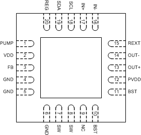
 Figure 5-1 RGP Package20-Pin QFN With Exposed
Thermal PadTop View
Figure 5-1 RGP Package20-Pin QFN With Exposed
Thermal PadTop ViewTable 5-1 Pin Functions
| PIN | TYPE | DESCRIPTION | |
|---|---|---|---|
| NAME | NO.1 | ||
| PUMP | 1 | P | Internal charge pump voltage |
| VDD | 2 | P | 3- to 5.5-V supply input. A 1 µF-capacitor is required. |
| FB | 3 | I | Boost feedback |
| GND | 4, 5, 6 | P | Supply ground |
| SW | 7, 8 | P | Internal boost switch pin |
| NC | 9 | — | No connect |
| BST | 10, 11 | P | Boost output voltage. A 0.1-µF capacitor is required. |
| PVDD | 12 | P | High-voltage amplifier input voltage |
| OUT+ | 13 | O | Positive haptic driver differential output |
| OUT- | 14 | O | Negative haptic driver differential output |
| REXT | 15 | I | Sets boost current limit. Resistor to ground. |
| IN- | 16 | I | Negative analog input |
| IN+ | 17 | I | Positive analog input |
| SCL | 18 | I | I2C clock |
| SDA | 19 | I/O | I2C data |
| REG | 20 | O | 1.8-V regulator output. A 0.1-µF capacitor is required. |
- I = Input, O = Output, P = Power